Update (2026-11): the features below shipped in WireFrame 2.0.1–2.0.3, and AI layout with
/layoutfrom the "Still being built" list is out too; the current release is 2.0.4 — download, release notes.
The public download of WireFrame EDA is still v1.3.8: schematic capture, PCB layout, 3D, DRC/DFM and fabrication output. Everything below is in the 1.5.x beta builds that become the next release. This is where the work stands on 20 October 2026, and what is still being built.
The AI Copilot, measured#
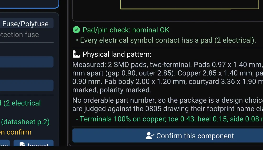
We drove the real Copilot panel end to end on 20 designs of 36 to 106 parts (up to 597 pins: microcontrollers, an FPGA, SDRAM and eMMC, Ethernet, CAN and RS-485, a BLDC driver, a Raspberry Pi CM4 carrier). A written requirement became a checked BOM and netlist in 6 to 17 minutes, and no design was left with nothing it could draw.
What changed to get there:
- Placement review. Blocks are drawn with findings still open, each marked on the canvas with its number. Only a part the drawing would get wrong holds its block back.
- Your edits flow back. Change a value, a footprint or a wire on the sheet and the BOM plan and netlist follow — and the repair agents are told never to undo it.
- It knows what you changed. A change that keeps the checks green is your decision and is never reverted; one that breaks a check is pointed out and asked about.
/referencelifts a part's support circuit from a built KiCad or Altium design, with the source's licence named.- WireFrame AI. The Copilot runs on WireFrame AI and your plan's AI credit, with nothing to set up.
Signal and power integrity, with the evidence#
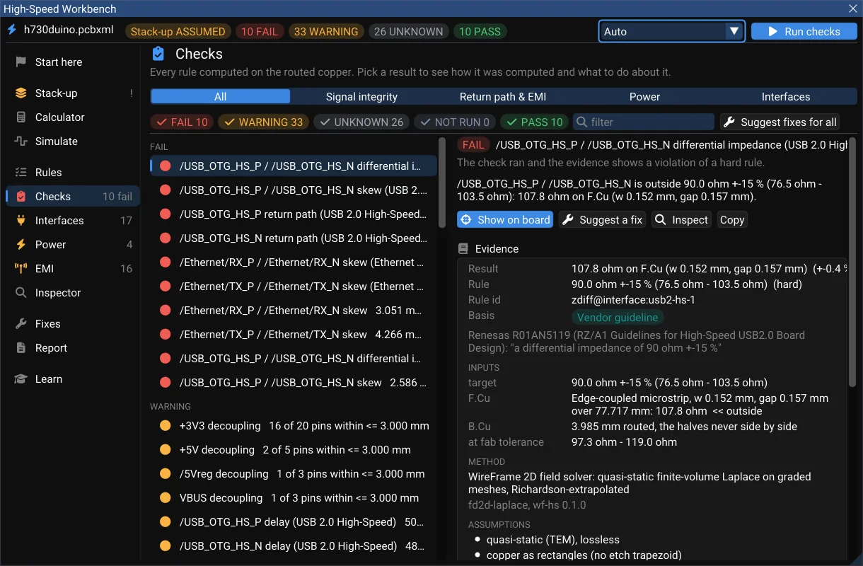
The biggest addition of the month is a High-Speed Workbench: impedance with a 2D field solver, differential-pair skew and length or time matching, return paths and plane edges, crosstalk, decoupling, PDN impedance and an EMI estimate against CISPR 32 and FCC — all computed on the copper you routed.
Two rules run through it. No PASS that cannot be proven: an unconfirmed stack-up caps every result at WARNING, and a missing input is UNKNOWN, never PASS. And nothing changes the board until a person approves it: fixes are previewed on a copy, approved, and applied as one undo step. Twelve interface profiles — USB 2.0 and 3.x, PCIe, Ethernet, HDMI, MIPI, LVDS, SATA, DDR3/DDR4, RGMII, QSPI, SD/eMMC — cite the document behind every row.
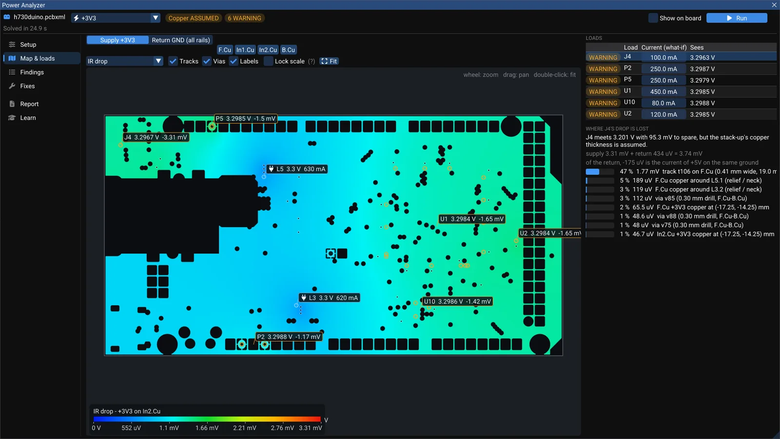
Beside it, a Power Analyzer solves DC IR drop on the real copper — supply and return, rails sharing a ground, the power tree, self-heating — and splits each load's drop exactly over the copper that causes it.
Read more: High-Speed Workbench · Power Analyzer · the guide.
Boards, views and routing#
- Multi-board products. One project, a PCB per board, and one assembly that checks every connection between boards pin by pin — including bought boards such as a Raspberry Pi, a BeagleBone or a sensor module. More.
- Schematic, board and 3D side by side, with cross-probing: a part picked in one view is highlighted in the other two.
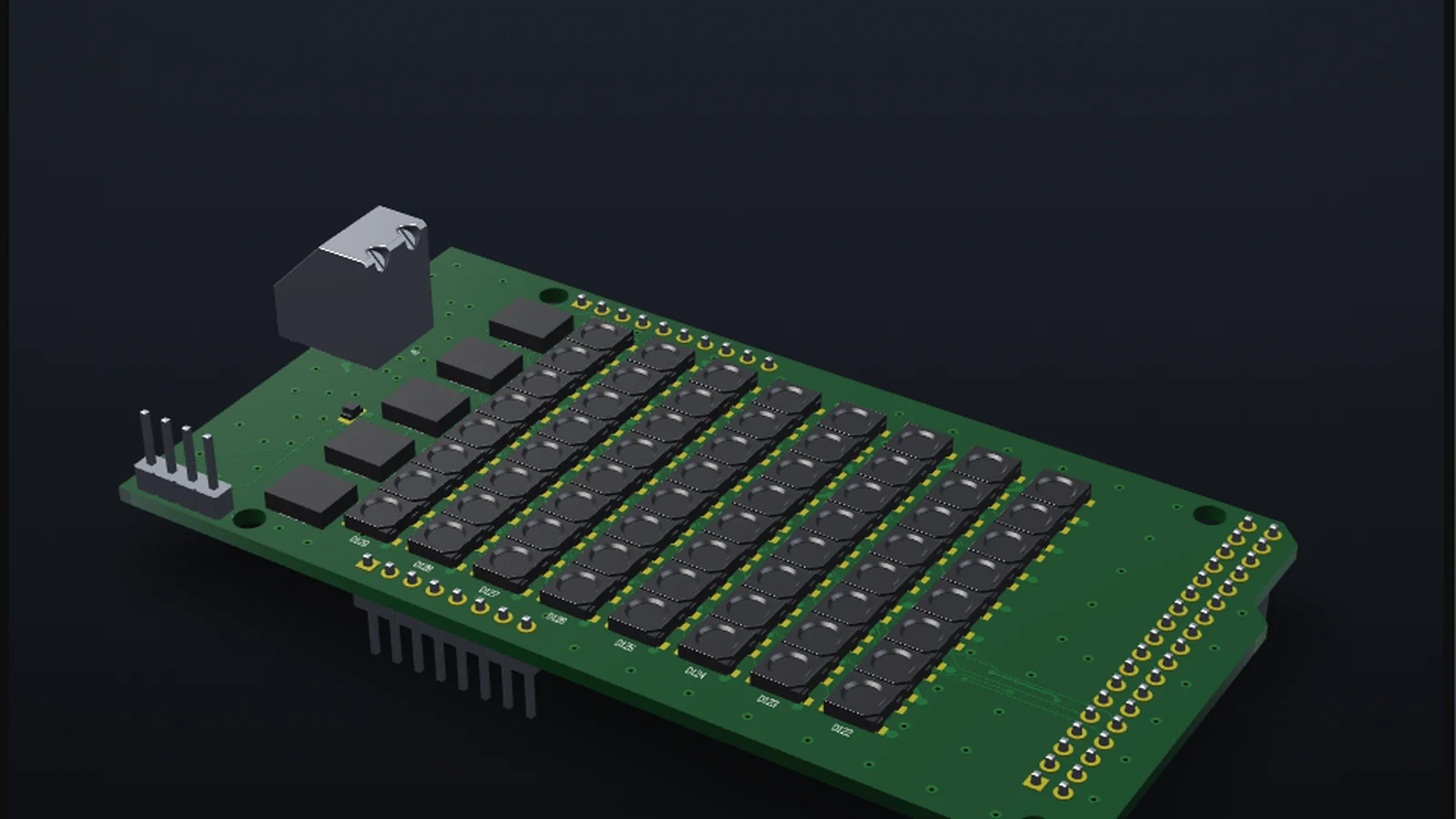
- A physically based 3D view with true STEP colours, mask colours and surface finishes.
- Free routing with Route Assist. A click lays exactly what the preview shows; clashes are drawn and reported instead of refused; Route Assist auto-routes a net or a bus, or reroutes only the clashing tracks, as one undo step.
Exchange#
File › Import › Altium Project joins the KiCad importer, and File › Export writes KiCad, Altium Designer and EasyEDA projects. Every export compares the nets the written files mean with WireFrame's own, pin by pin — measured with kicad-cli on boards of up to 3,050 pins with no net split and none merged. More.
Still being built#
- AI layout (
/layout): placement, planes, vias and routing streamed onto the canvas and applied only on your word. Written about here; not yet in a release. - Thermal and noise analysis from the layout itself.
- Logic levels across boards in assemblies (a 3.3 V host driving a 5 V input is not caught yet).
The release notes list every change: docs/changelog. If you want to try a beta build, or have a board you would like us to open, write to us from the sponsor and partner page.