PCB design, AI & WireFrame
Practical guides on board design, high-speed routing, moving from KiCad, sample boards and AI-assisted electronics.
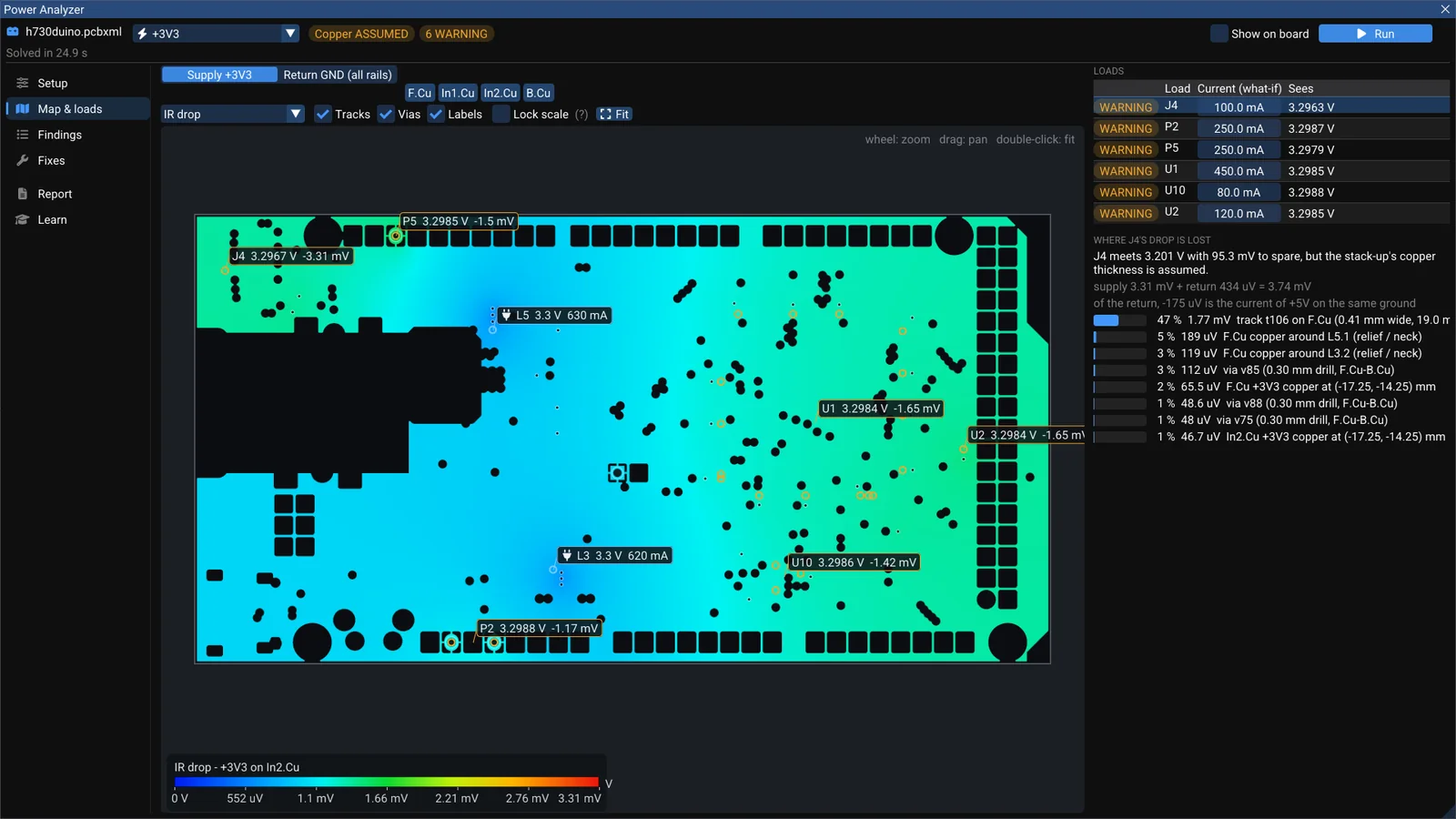
Where does your 3.3 V go? DC IR drop on a real board
WireFrame's Power Analyzer solves a rail's real copper — supply and return — and splits each load's voltage drop exactly over the tracks, necks and vias that cause it. A walk through the +3V3 rail of the open-source h730duino.
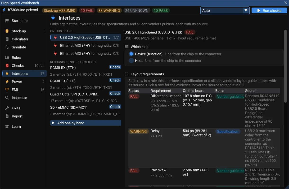
A USB pair at 107.8 Ω — high-speed checks that show their evidence
Running WireFrame's High-Speed Workbench on the open-source h730duino board — the USB 2.0 pair's impedance, skew and common mode, its EMI margin, and the fix — with the method and the source behind every number.
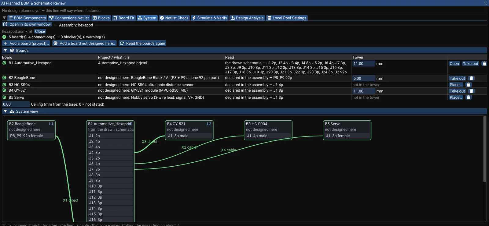
One product, many boards — every connection checked pin by pin
A HAT on a Raspberry Pi, a cape on a BeagleBone, a front panel on a cable — WireFrame treats a product of several boards as one project and checks every connection between them, bought boards included. Shown on an open-source hexapod robot's BeagleBone AI cape.
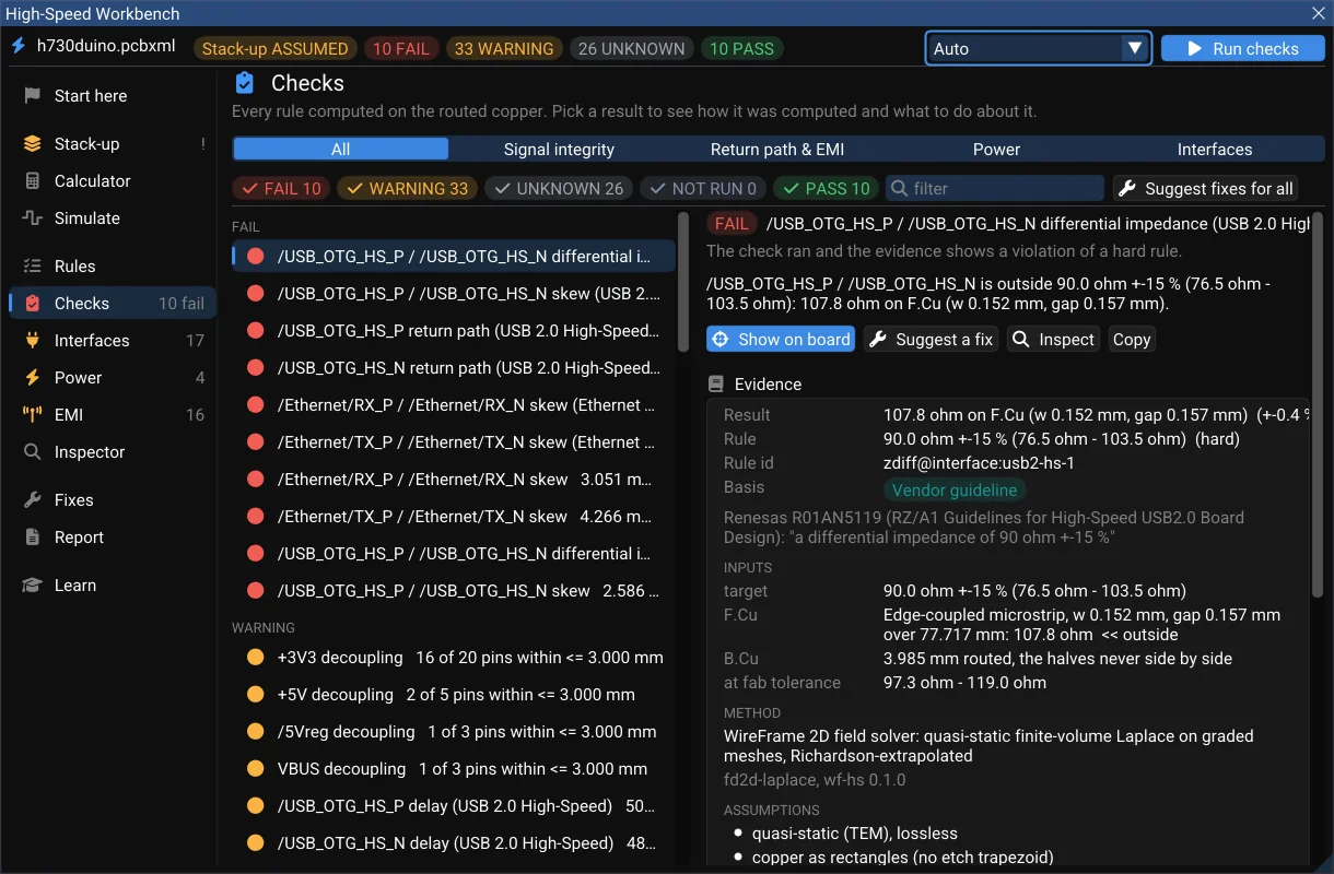
WireFrame EDA development update — October 2026
What WireFrame 2.0 brings, written in October 2026 before it shipped — the AI Copilot measured on 20 designs, a High-Speed Workbench and a Power Analyzer that show their evidence, multi-board products, KiCad/Altium/EasyEDA exchange, and what is still being built.
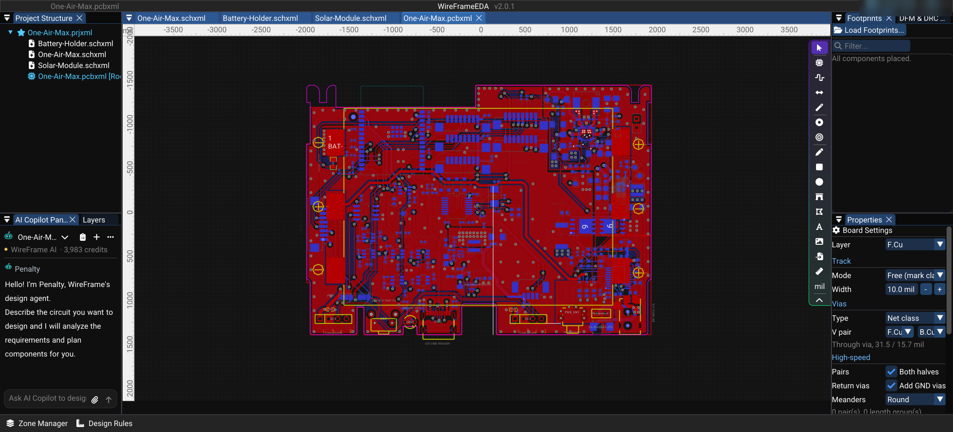
Sample board One-Air-Max — a 4-layer ESP32-C6 air-quality sensor with a PCB antenna, in WireFrame EDA
KiCad's One-Air-Max demo (ESP32-C6, solar and battery charging, buck converter, sensor front-end) imported into WireFrame EDA — its four-layer stackup and the keepout that keeps copper away from the antenna.
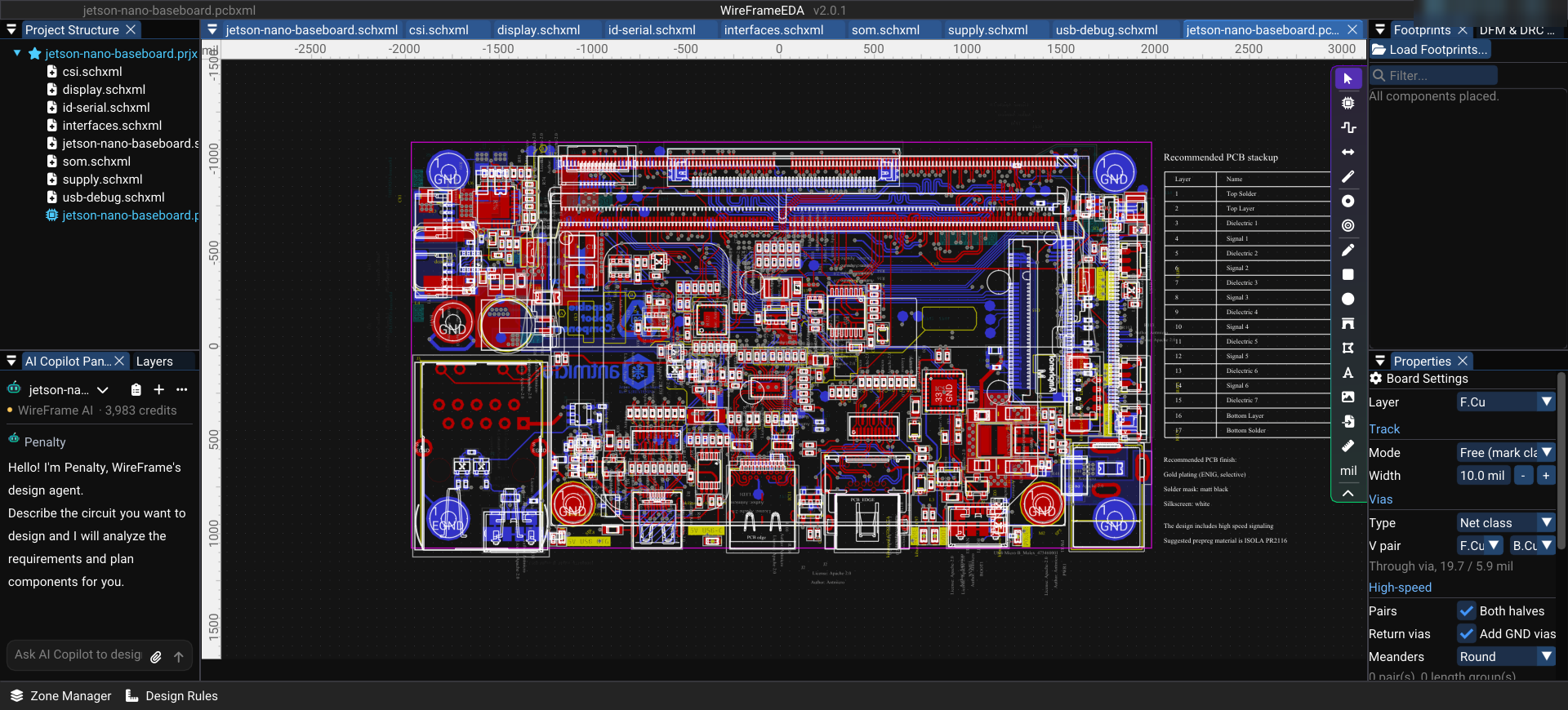
Sample board Jetson Nano baseboard — an 8-layer SO-DIMM carrier, opened in WireFrame EDA
Antmicro's open-source baseboard for the Jetson Nano and Xavier NX modules, imported from KiCad into WireFrame EDA — what is on its eight layers and what WireFrame measures on it.
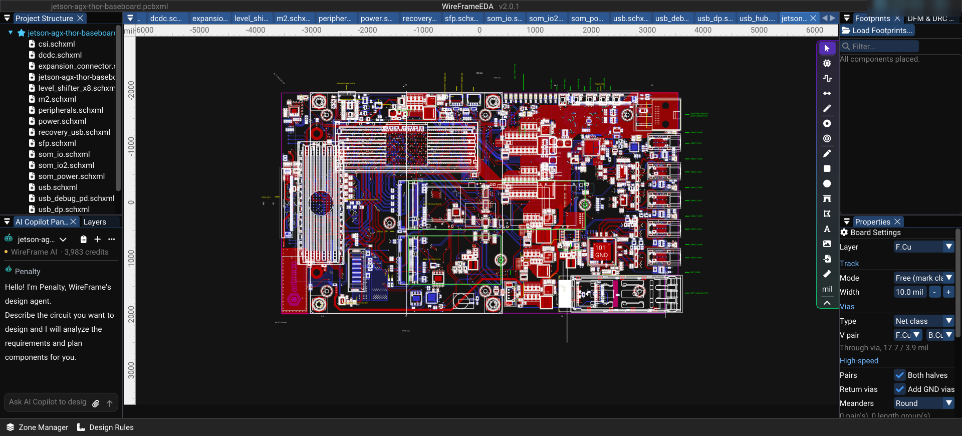
Sample board Jetson AGX Thor baseboard — 10 layers and 1124 parts, opened in WireFrame EDA
Antmicro's open-source carrier for the NVIDIA Jetson AGX Thor module, imported from KiCad into WireFrame EDA — its ten-layer stackup, length-tuned camera pairs and the numbers WireFrame measures on it.
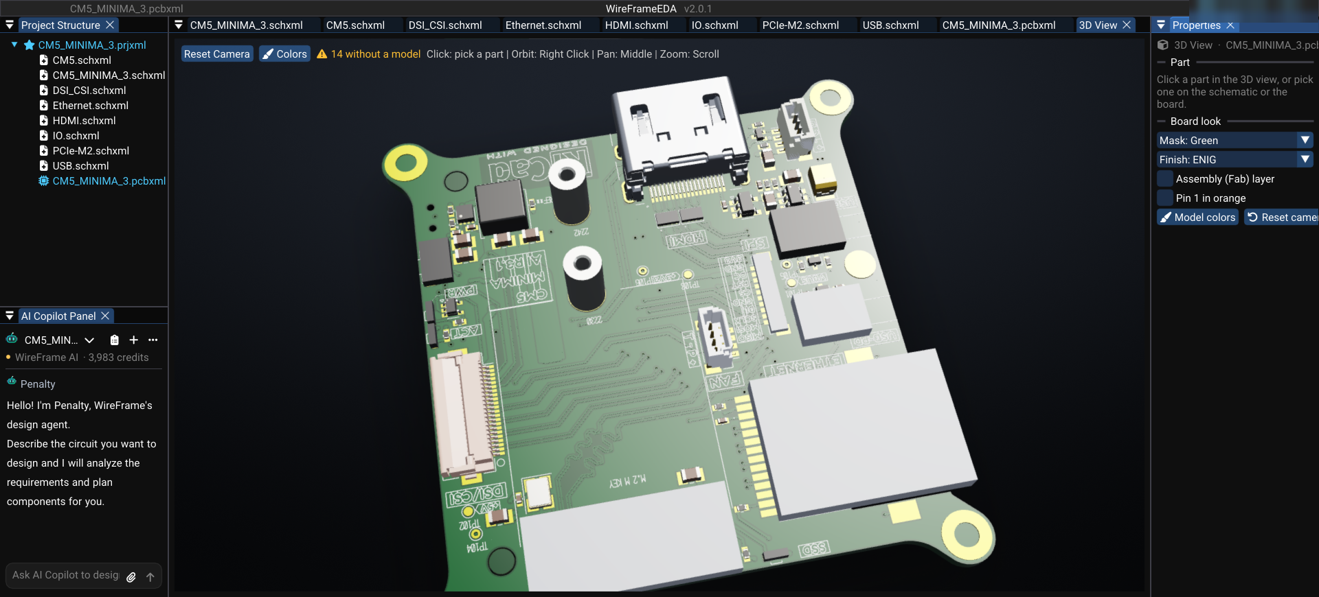
Sample board CM5 Minima — a 6-layer Raspberry Pi CM5 carrier, in 2D and 3D in WireFrame EDA
The CM5 Minima carrier for the Raspberry Pi Compute Module 5, from KiCad's demo projects, imported into WireFrame EDA — four inner planes, an M.2 slot, and the parts drawn from their 3D models.
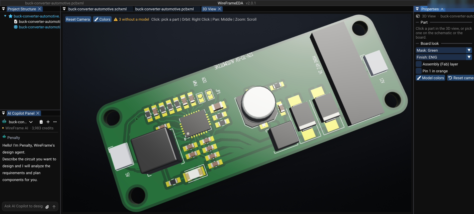
Sample board automotive buck converter — 12 V to 5 V on two layers, in WireFrame EDA
A small open-source MAX17574 buck converter for 12 V vehicles, imported from KiCad into WireFrame EDA — fully routed, ground poured on both sides, clean DRC, and what to look at on a board this size.
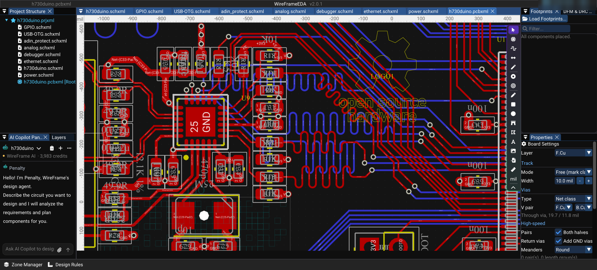
Length matching in practice — RMII and SDMMC on the H730duino
Measuring the real routed lengths of the RMII Ethernet and SDMMC traces on the open-source H730duino board: seven RMII signals matched within 0.02 mm. Why, and when you don't need to.
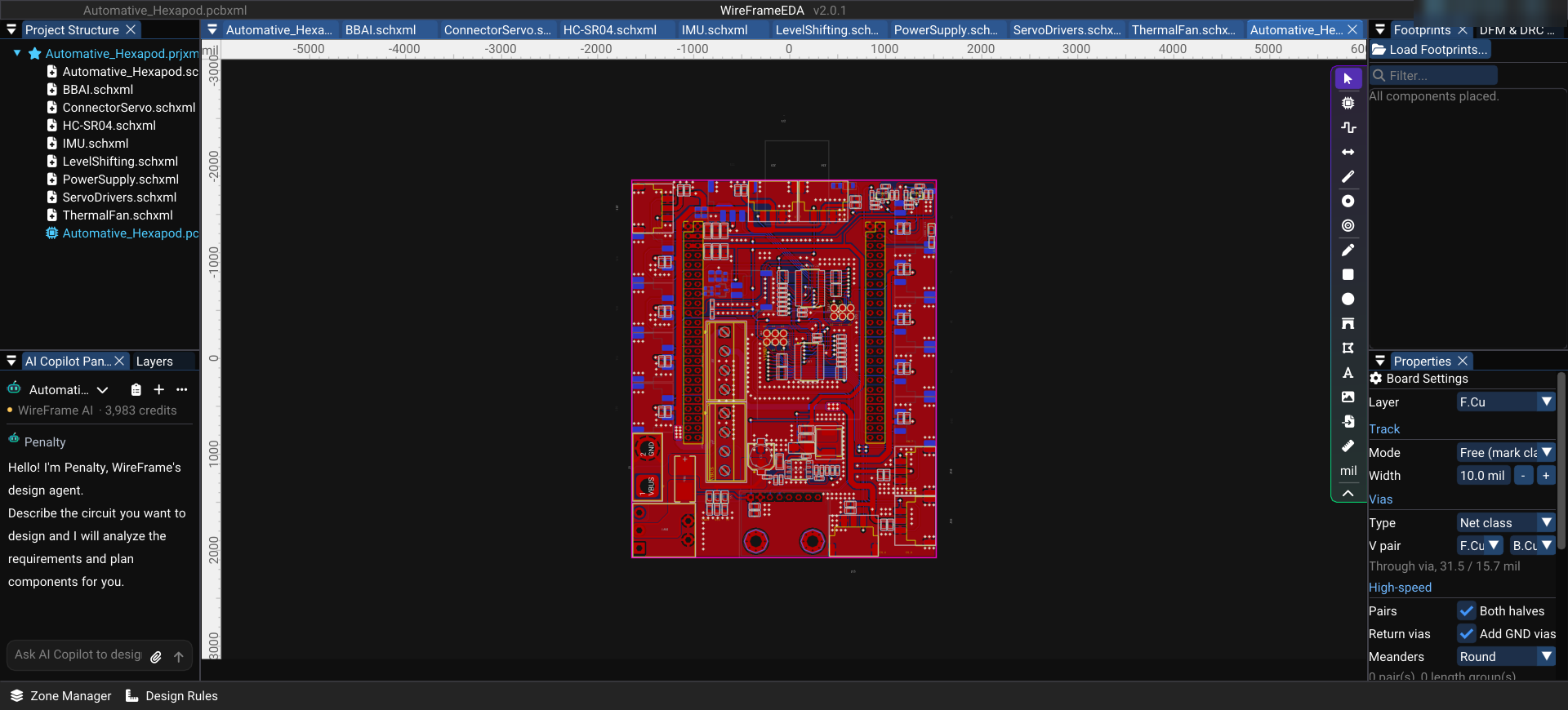
Hardware design walkthrough: 18-servo hexapod robot main board on BeagleBone AI
Reading the main board of the open-source reinforcement-autonomous-hexapod robot: BeagleBone AI, two PCA9685 driving 18 servos, an MPU6050 IMU, an ultrasonic sensor and a TPS54331 supply — opened in WireFrame EDA.
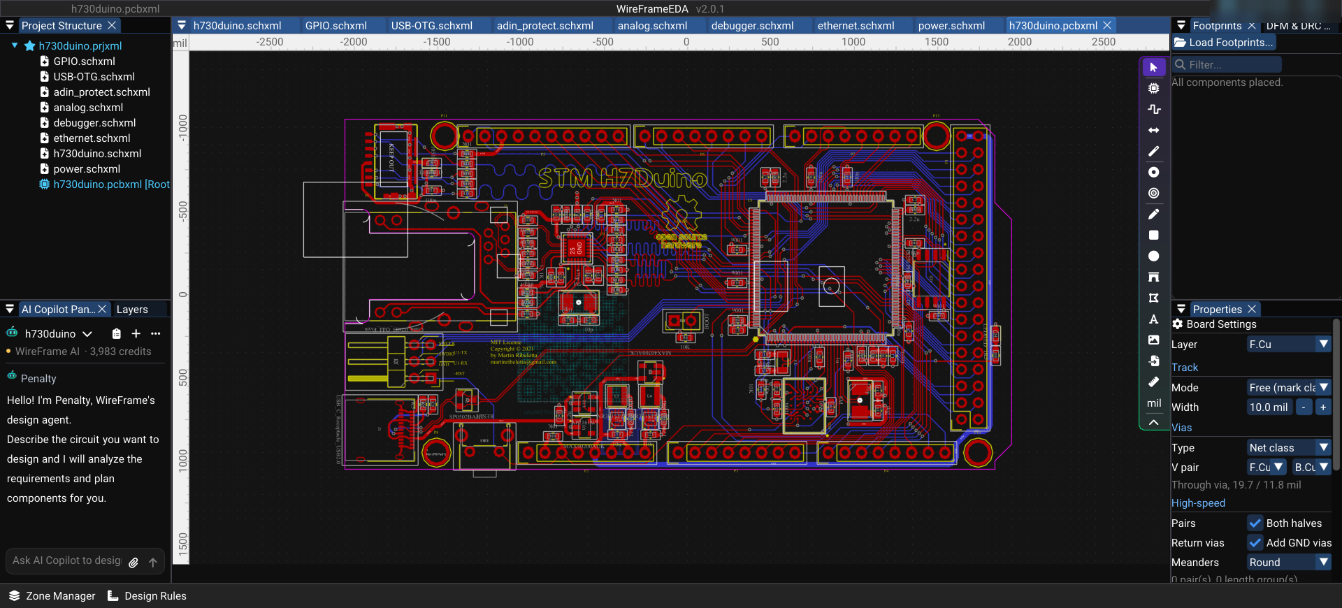
Sample board H730duino — a 4-layer STM32H730 Arduino Mega-format board, opened in WireFrame EDA
Opening the open-source KiCad project H730duino (STM32H730, Ethernet, HyperRAM, USB-C) in WireFrame EDA to read its 4-layer stackup, GND/3V3 planes, length-matched meanders and board metrics.
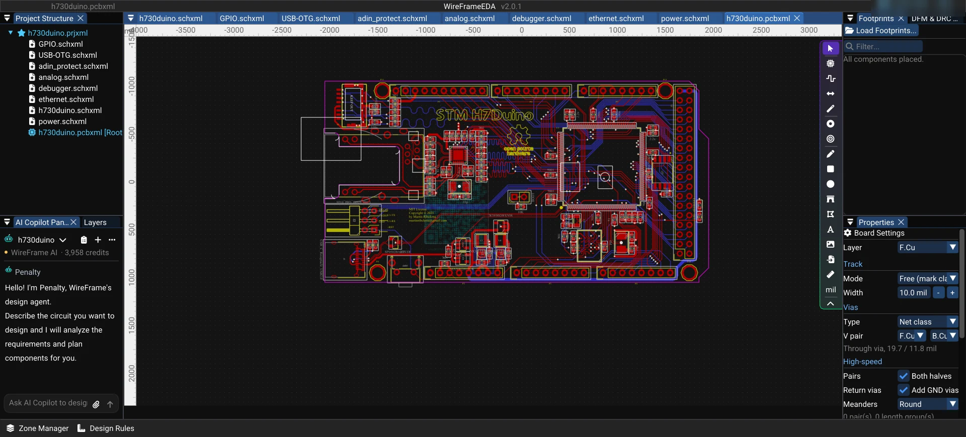
What is WireFrame EDA? A modern AI-assisted PCB design tool
WireFrame EDA is a desktop PCB design application for Windows, macOS and Linux — schematic, layout, 3D, Gerber export and SPICE simulation — with an AI Copilot (Pro and Max) that drafts schematics from a description.
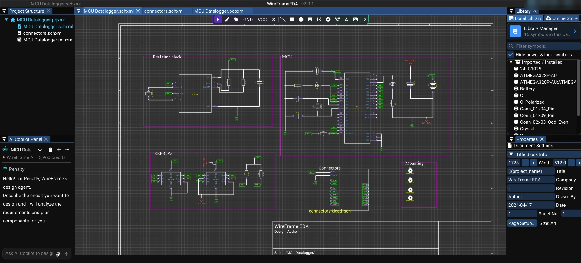
Moving a KiCad project to WireFrame EDA — libraries, schematics and PCB
How to open a KiCad project (.kicad_pro) in WireFrame EDA, reuse your KiCad symbol and footprint libraries, and what to check after the move.
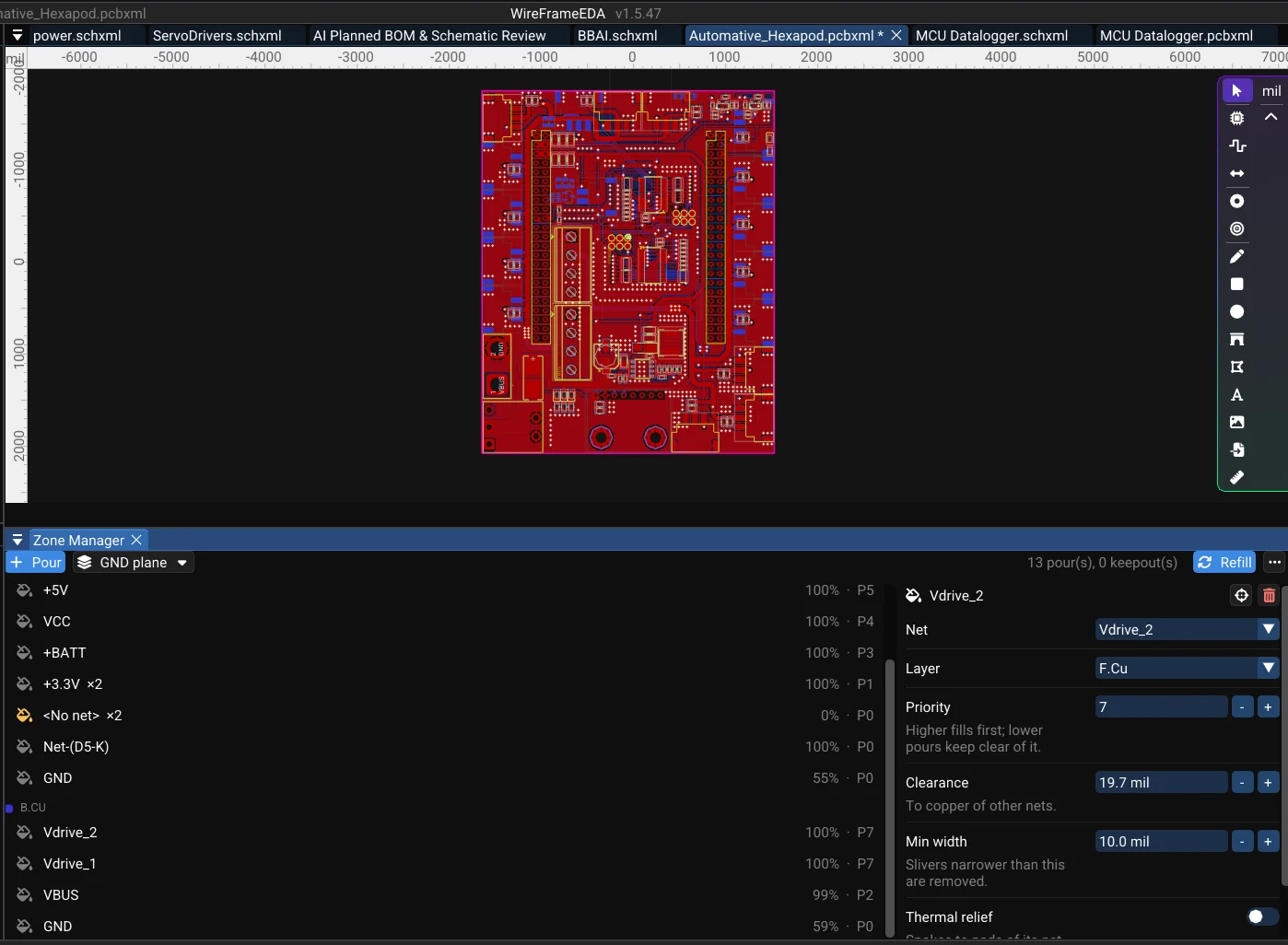
Choosing a 4-layer PCB stackup for microcontroller boards — SIG/GND/PWR/SIG or SIG/GND/GND/SIG?
The two common 4-layer stackups explained, with return paths, ground stitching vias, decoupling and antenna keepouts — and how to set them up in WireFrame EDA.