Short answer: File ▸ Import ▸ KiCad Project opens a KiCad project — KiCad 5 .pro up to current .kicad_pro — as a WireFrame project, and File ▸ Export ▸ KiCad Project… writes it back. Both directions are measured. On the KiCad demo projects WireFrame was measured against, the imported connectivity is identical to kicad-cli's own netlist — 15 of 15 projects. On 36 of the demo projects that ship with KiCad, all 72 round trips — 36 through KiCad, 36 through Altium Designer — come back identical. Import and export are part of the free design tools.
The earlier post Moving a KiCad project to WireFrame EDA covered the way in. This one covers both directions and how the numbers were measured.
Why measure the way back?#
An import that drops one net is worse than no import at all, because you find out when the boards come back. And a tool you cannot leave is a tool you should not adopt. So WireFrame's exchange is tested by comparison with the other tool, not judged by eye, and the export is held to the same comparison as the import.
Step 1: open the KiCad project#
- Select File ▸ Import ▸ KiCad Project (.kicad_pro, .pro)…
- Pick the
.kicad_profile (KiCad 6 and later) or the.profile (KiCad 5). - Keep WireFrame open while the progress overlay reports each import stage. The WireFrame project — a
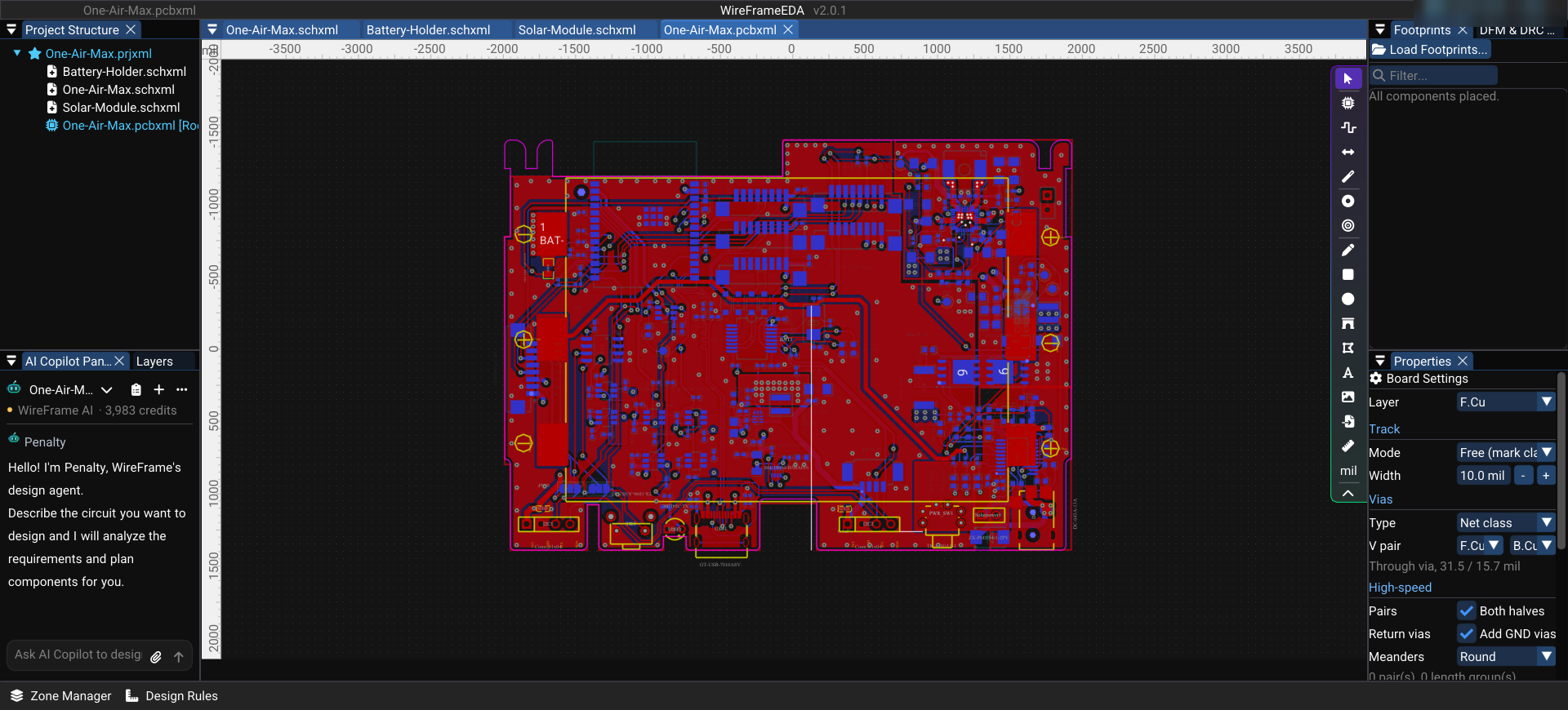
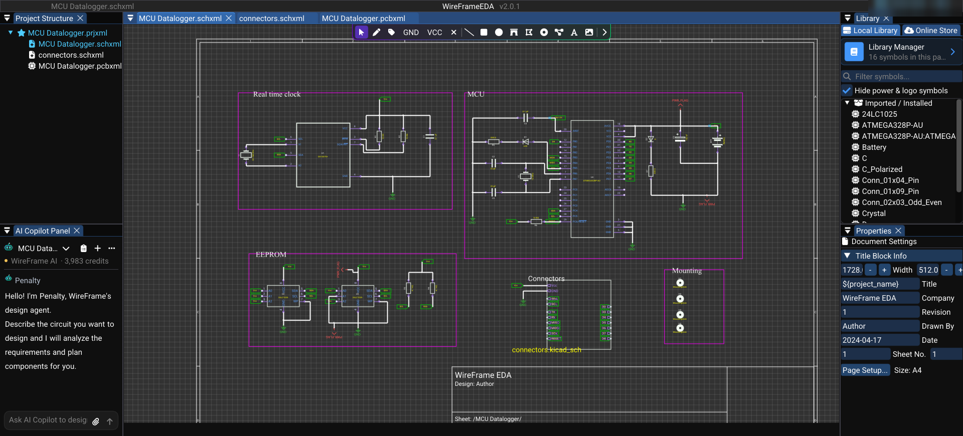
.prjxmlwith its.schxmlsheets,.pcbxmlboard and project library — is written into the KiCad project's folder. Your KiCad files are not modified. - Review the project, the sheets, the board and the library assignments, then save.
What comes across: the sheets, hierarchical and flat, with sub-sheets used more than once; the board; the project's own libraries and 3D model paths; net classes; the design and fabrication constraints from the project's setup (the fab preset becomes Custom with KiCad's values); the stack-up, zones, arcs (kept as arcs) and vias with KiCad's remove unused layers. Schematic pages keep their real size. A KiCad 10 project's design variants come in too, and the project's custom rules (.kicad_dru) are read as far as WireFrame understands them; the rest are named under W19 in the DRC list, so a clean list is not mistaken for "every rule passed".
KiCad libraries need no conversion at all. WireFrame reads .kicad_sym and .kicad_mod files in place, so there is no second copy of your library to go stale.
Keep reading — it’s free
Sign in or create a WireFrame account to read the rest of this post and every guide on the blog.
- The rest of this post — about 4 min of reading
- The same account signs in the WireFrame desktop app
- Free design tools, no time limit
Sign in to WireFrame
One account for the desktop app and this site.