PCB design, AI & WireFrame
Practical guides on board design, high-speed routing, moving from KiCad, sample boards and AI-assisted electronics.
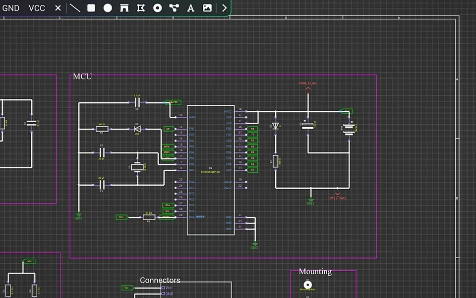
KiCad to WireFrame EDA and back: 72/72 round trips identical
Open a KiCad project in WireFrame EDA, work on it and export it back to KiCad: what comes across, what to check, and how the round trip was measured.
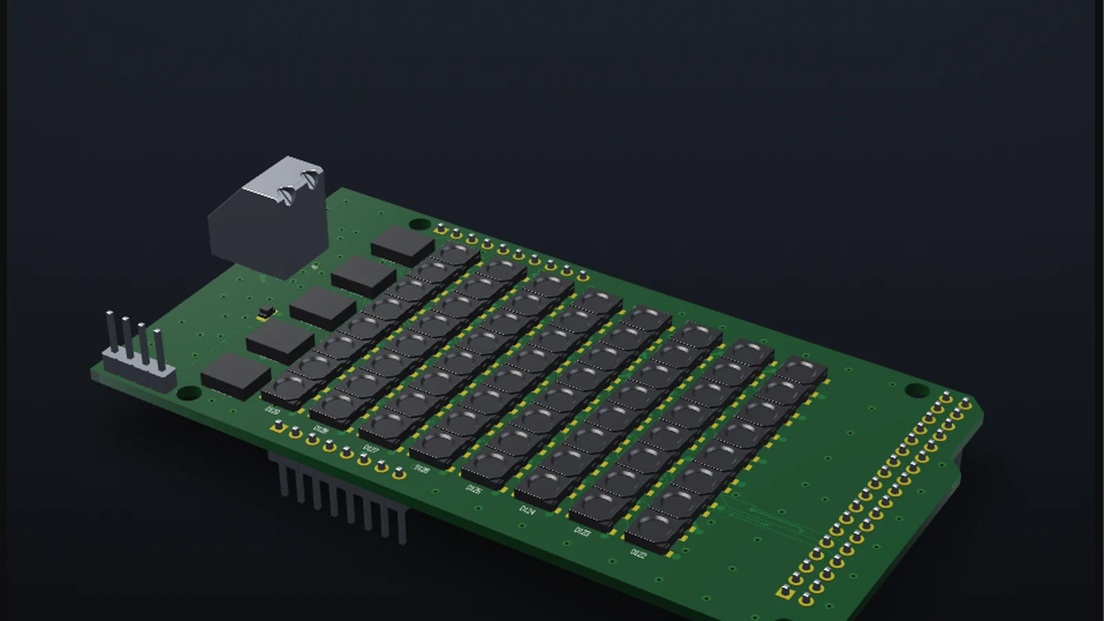
How to design a PCB with Claude over MCP in WireFrame EDA
Connect Claude, Codex or Cursor to WireFrame EDA over MCP and let your own agent design the board you have open: setup, the Allow step, what is counted.
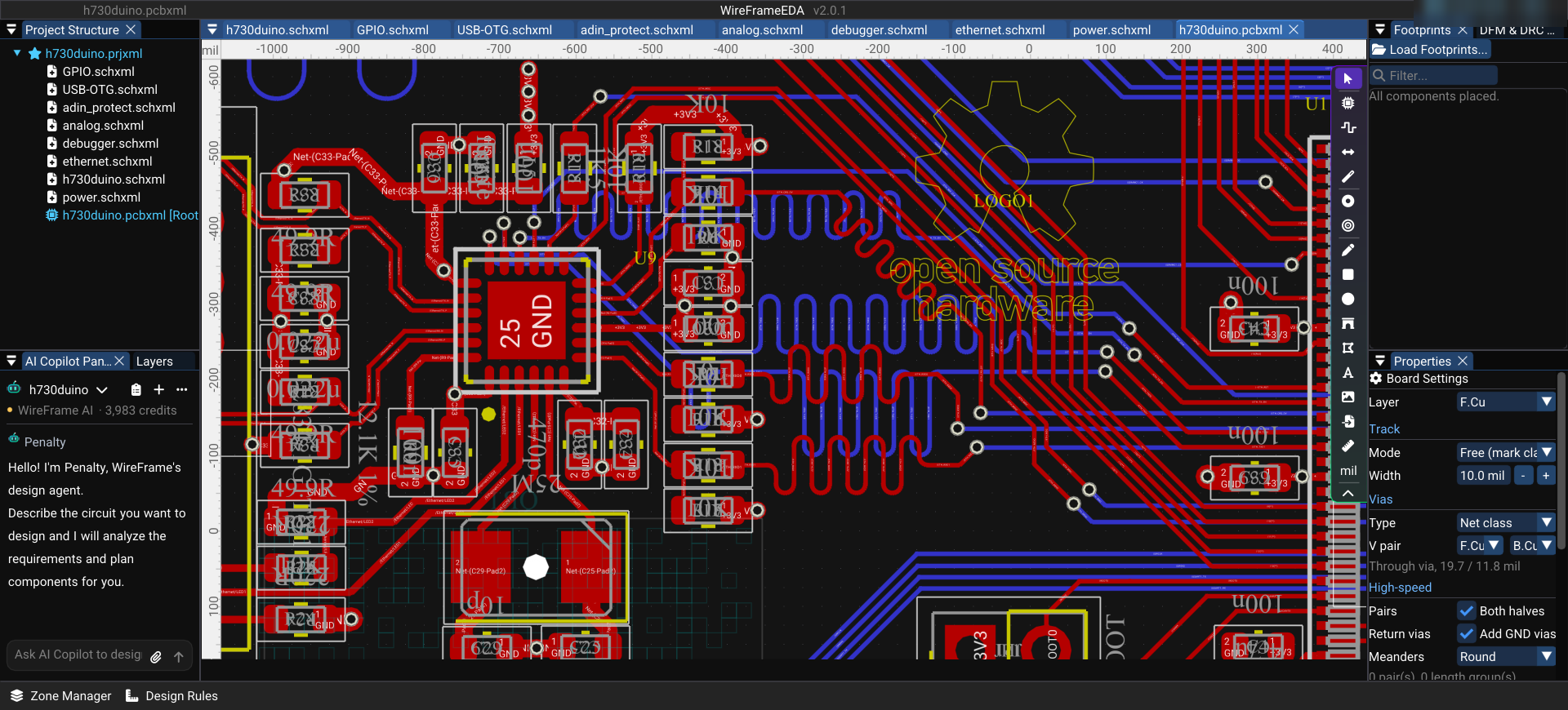
Length matching in practice — RMII and SDMMC on the H730duino
Measuring the real routed lengths of the RMII Ethernet and SDMMC traces on the open-source H730duino board: seven RMII signals matched within 0.02 mm. Why, and when you don't need to.
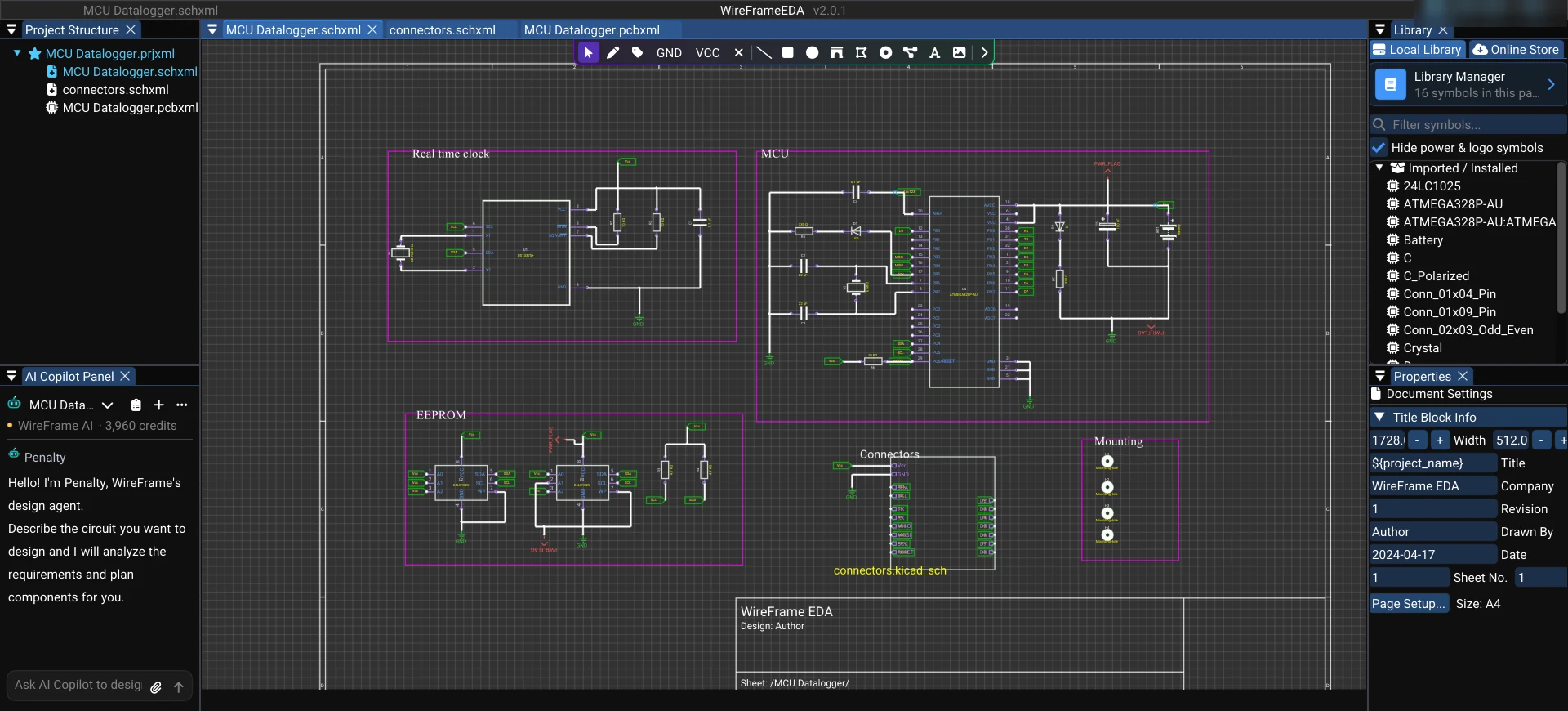
Moving a KiCad project to WireFrame EDA — libraries, schematics and PCB
How to open a KiCad project (.kicad_pro) in WireFrame EDA, reuse your KiCad symbol and footprint libraries, and what to check after the move.
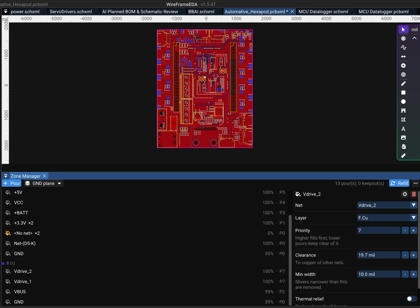
Choosing a 4-layer PCB stackup for microcontroller boards — SIG/GND/PWR/SIG or SIG/GND/GND/SIG?
The two common 4-layer stackups explained, with return paths, ground stitching vias, decoupling and antenna keepouts — and how to set them up in WireFrame EDA.
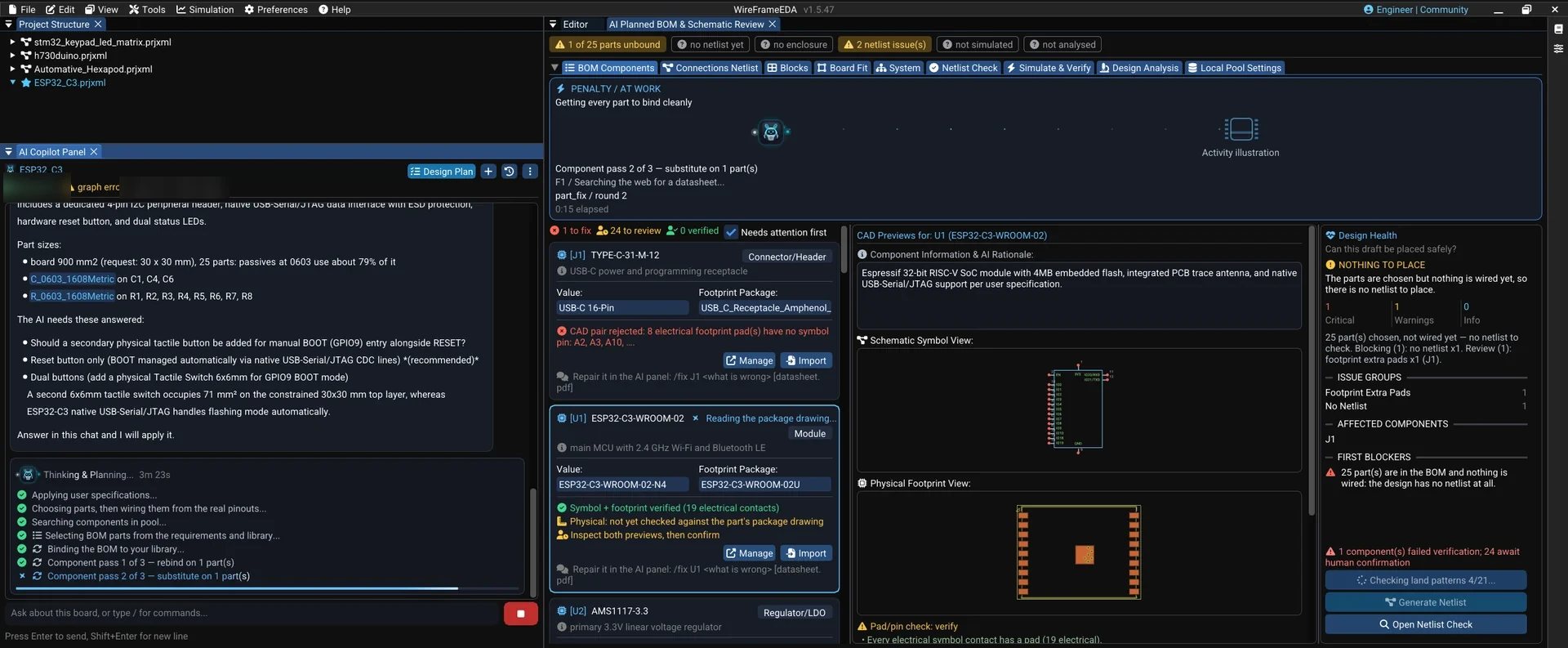
WireFrame's AI Copilot — from a sentence to a datasheet-checked schematic
How the WireFrame EDA AI Copilot turns a written requirement into a BOM, netlist and schematic built from real parts, checks packages and pin maps against datasheets, and repairs rows with /fix.