3D, mechanics & products
3D Viewer
On this page
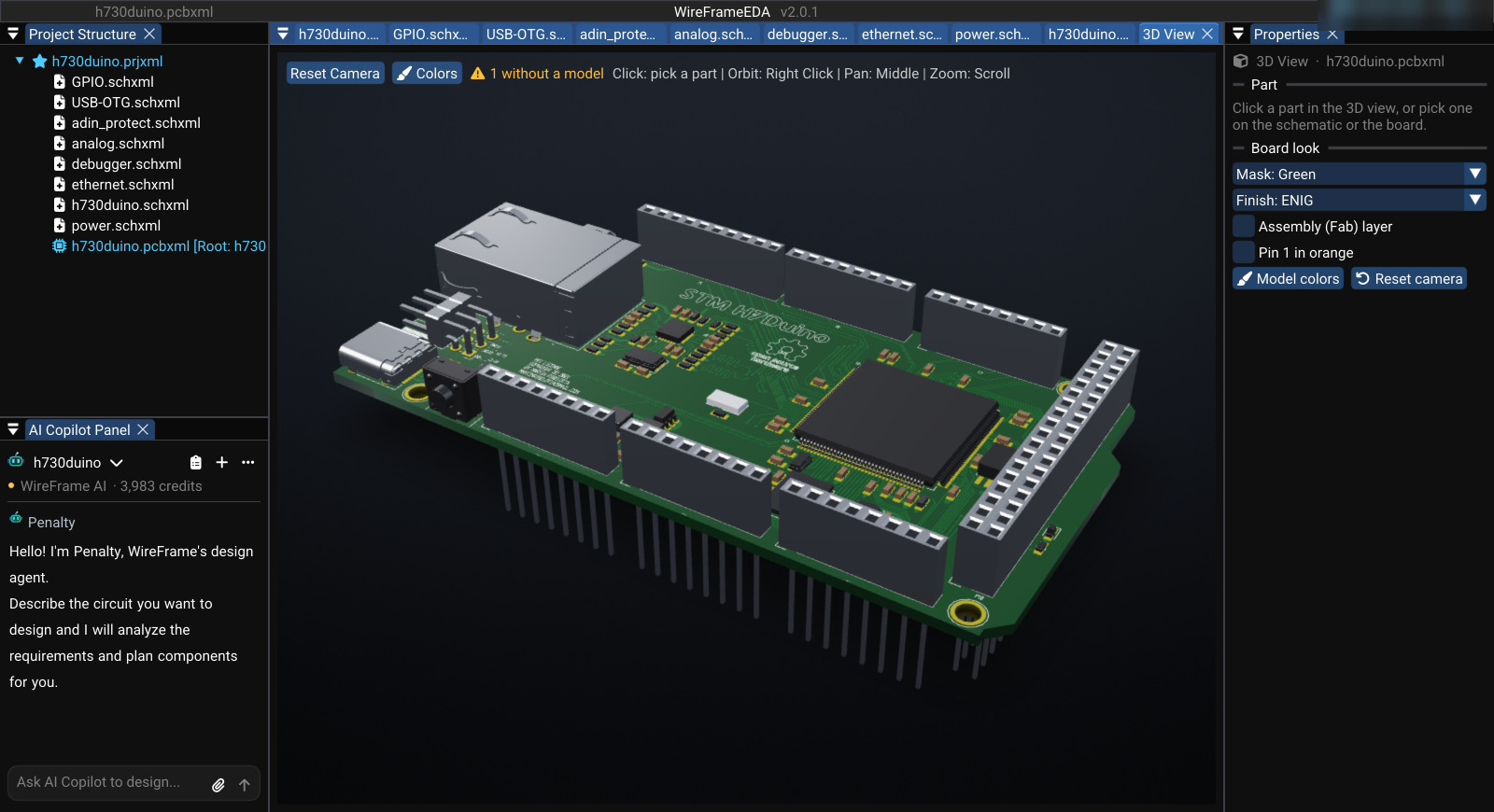
The 3D Viewer renders a three-dimensional representation of your PCB — showing component placement, board geometry, and spatial relationships — so you can validate your design before manufacturing.
Opening the 3D Viewer#
From an open PCB document:
- Go to View → 3D Viewer, or press 3 with the PCB active
- The 3D View panel opens; to make room, the Design Rules, Zone Manager, Layers, and DFM panels are closed
- It renders:
- The board as a 3D extruded shape derived from the Edge.Cuts outline
- Footprints with 3D models (STEP/OBJ) if available
- Simple colored boxes for footprints without 3D models
Camera Controls#
| Action | Input | Effect |
|---|---|---|
| Pick a part | Click without dragging | Selects nothing — it probes the part: boxed and labelled here, ringed on the board and the sheet |
| Orbit | Right mouse button drag | Rotate the camera around the board |
| Pan | Middle mouse button drag | Move the camera parallel to the screen |
| Zoom | Mouse scroll wheel | Zoom in / out |
| Reset | Reset Camera, or Home | Back to the default three-quarter view, framed on the board and its parts |
The toolbar shows Reset Camera, Colors (load the models' full STEP colours), a count such as ⚠ 1 without a model, and the hint Click: pick a part | Orbit: Right Click | Pan: Middle | Zoom: Scroll. Hovering a part names it.
The view always shows the board you are working on (or the last one), so it can stay open beside the schematic — see Schematic, Board and 3D Side by Side. While you drag a footprint on the board, the 3D view follows it.
How It Looks#
The viewer renders physically: metals reflect, the mask has depth, the light follows the camera, edges are anti-aliased, and the board sits on a soft shadow like a product shot. STEP colours are read as the model's author set them.
Board look — in the 3D view's Properties while the view is in front, and in Preferences → 3D Viewer, saved with the session:
| Setting | Choices |
|---|---|
| Mask | Green (default), red, blue, black, white, purple… |
| Finish | ENIG, HASL or bare copper — the colour of exposed pads |
| Assembly (Fab) layer | Show the fabrication layer's outlines and designators |
| Pin 1 | Highlight pin 1 of every part in orange |
Silkscreen is clipped to the board outline, so a connector's outline hanging over the edge does not float in the air.
How Components Are Rendered#
With a 3D model (STEP / OBJ)#
- The actual 3D mesh from the STEP or OBJ file is rendered
- Colors and materials come from the model file
Without a 3D model#
- A simple colored bounding box approximating the footprint size is drawn
- Color is determined by the designator prefix:
| Prefix | Color | Component type |
|---|---|---|
| R | Beige | Resistor |
| C | Dark grey | Capacitor |
| L | Dark grey | Inductor |
| U | Near-black | IC |
| J, P | Green | Connector |
| D | Orange-red | Diode |
| Q | Black | Transistor |
| S | Red | Switch |
| H | Tan | Mechanical hole |
Board materials — solder mask, finish, silkscreen — are set as described in How It Looks.
Bottom-Side Components#
Footprints flipped to B.Cu are rendered on the underside of the board with the same orientation shown in the 2D editor.
Use the underside camera view to confirm that flipped models, silkscreen, pad plating, and board clearances match the 2D layout.
Practical Use Cases#
| Use case | How |
|---|---|
| Verify component placement | Orbit around the board, zoom into areas of interest |
| Check physical clearances | Zoom into tall components (connectors, relays) to check they don't interfere |
| Inspect bottom-side components | Orbit below the board to view B.Cu placement |
| Capture for documentation | Position the view and take a screenshot with your operating system's tool |
| Hand the board to the case designer | Board Fit's Export for the case (STEP)… — see Enclosure Fit |
STEP files load slowly the first time
First-time loading of STEP files may take several seconds due to mesh tessellation and GPU upload. Subsequent frames use the cached mesh and are fast.
Assigning 3D Models to Footprints#
To display an accurate 3D model instead of a coloured box, attach a STEP model to the footprint:
- Open View → Local Library Manager, select the part, and open its 3D tab
- Choose Edit 3D model & alignment
- In Model Alignment, use Import 3D File..., adjust Translation, Rotation, and Scale, then Save to .kicad_mod
See: Footprint Libraries — Align a 3D model
In a 3D preview (Library panel or Library Manager), Load Colors reloads the model with its full STEP colours (slower), No Model means the footprint has none, and Load Failed means a model file could not be read.
See Also#
- PCB Editor — the 2D PCB workspace
- Schematic, Board and 3D Side by Side — cross-probing
- Multi-Board Products — the Assembly 3D of a tower of boards
- Fabrication & Export — export after 3D verification