Libraries
Footprint Libraries
On this page
Footprints define the physical pads, drills, component outline, and optional 3D model used on the PCB. Select the exact manufacturer package and recommended land pattern, not only a similarly named footprint.
Add a footprint source#
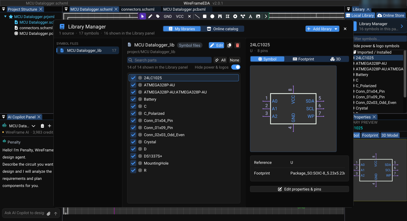
- Open View → Local Library Manager.
- Select Add library ▾ → Folder of KiCad libraries... and choose the folder with
.kicad_modfiles or.prettyfolders. - Select the source and confirm its footprints are listed.
- Assign footprints to symbols (see Symbol Libraries); the PCB receives them through Update Schematic to PCB.
Keep custom footprints and their 3D models in a controlled project or team location so another machine can resolve them.
Review a footprint#
Compare the footprint with the exact datasheet land pattern:
- package name and body dimensions;
- pad count, numbering, shape, size, and pitch;
- plated or non-plated drill geometry;
- pin-1 or polarity marker;
- solder-mask and paste behavior;
- courtyard, silkscreen, and fabrication outlines;
- component origin and board-side orientation;
- symbol-pin to footprint-pad mapping.
Print or measure at 1:1 scale when dimensions are safety-critical. A 3D model is useful for review but does not prove that the pads are correct.
The Footprint Library Editor#
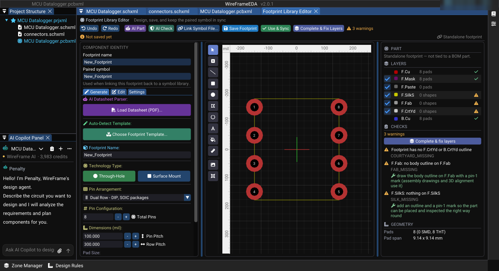
Open Tools → PCB Footprint Editor (or Edit in the Footprint Editor from the Library Manager). The Footprint Library Editor opens as a tab — Design, save, and keep the paired symbol in sync.
Before release, place the footprint on a test board and inspect pad geometry, courtyard, silkscreen, origin, and orientation.
Layout of the editor#
| Area | Contents |
|---|---|
| Top bar | Undo, Redo, AI Part, Link Symbol File..., Save Footprint, Use & Sync, and — when layers are missing — Complete & Fix Layers, with a status such as Not saved yet or Geometry valid |
| Component identity | Footprint name (required, e.g. SOIC-8) and Paired symbol (optional — used when linking back to a symbol library) |
| Left tabs | Generate, Edit, Checks, Settings |
| Canvas | Tool strip, pads and graphics, rulers, the unit button (mil / mm) |
| Right panel | Part, Layers (pads or shapes per layer, with a warning when a layer is empty), Checks, Geometry (pad count, pad span) |
Generate a footprint from parameters#
On the Generate tab:
- Under Auto-Detect Template, choose Choose Footprint Template... for a standard package. Templates are grouped — through-hole packages and sockets, SOIC/SOP, QFP/QFN/BGA, transistors and diodes, passives, crystals, connectors, switches and relays, LEDs, battery and high-current, RF modules and debug, mechanical utilities, standard pin headers.
- Or set the parameters yourself:
- Technology Type — Through-Hole (DIP, SIP, headers) or Surface Mount (SOIC, QFP, 0805…);
- Pin Arrangement — Single Row, Dual Row, Grid / Matrix (BGA, PGA), or Quad (QFP);
- Pin Configuration — Total Pins, or Rows and Columns for a grid;
- Dimensions — pin pitch (100 mil = 2.54 mm is the standard header pitch), row pitch, Pad Size, drill diameter (typically 0.8–1.0 mm), silkscreen margin, and body corner radius.
- The preview updates as you type. Override with Parametric Generator replaces a template with the parametric result.
Generate a footprint from a datasheet#
- On the Generate tab, under AI Datasheet Parser, select Load Datasheet (PDF)..., then Analyze For Footprint Pages.
- Optionally type Target Part Number / Package and select AI: Auto-Generate Parameters.
- Read the AI PACKAGE DECISION — its assumptions and checks — or select Open Manual Editor to draw the pads yourself.
- Select Review AI result. AI Footprint Evidence Review overlays the generated copper on the datasheet land pattern (Opacity, Scale, Rotate, Reset alignment; drag to align, wheel to scale) and lists where each value came from.
- Tick the REQUIRED HUMAN CHECKS — Pin 1 and orientation match, Shell tabs, holes and omitted balls match, Critical pitch and pad sizes match dimensions — then Approve & Apply (or Apply for manual editing).
Until the AI result is approved, the top bar reads Confirm AI review to Save/Sync.
AI Part on the top bar builds the whole part — footprint with every layer completed — from the datasheet's mechanical drawing.
Edit pads and graphics#
On the Edit tab (Manual Pad Editor):
- Add Pad (at the origin), Duplicate, Clear All; the Pad List shows every pad;
- select a pad to edit its Number, size, position, Rotation, Round/Oval Shape, and drill; Delete Selected Pad(s);
- graphics have a Layer, Fill Style, Content and Angle for text, and Convert to Rectangle for four-point polygons; Delete Selected Graphic;
- Display Unit: mil / mm switches the unit.
The canvas tool strip has Select & Move, Place Pad, Draw Line, Draw Rectangle, Draw Circle, Draw Polygon, Draw Arc, Draw Text, Flood Fill (Boundary Fill), Measure Distance, Import Image (Vectorize), and Fit footprint to canvas. Footprint geometry is stored in millimetres.
Checks and completing layers#
The Checks tab and the right panel list problems such as a missing courtyard (COURTYARD_MISSING), no fabrication body outline (FAB_MISSING), nothing on silkscreen (SILK_MISSING), SMD pads without mask or paste openings, paste on through-hole pads, or silkscreen too close to a pad. Most come with a hint.
Complete & Fix Layers adds what the fab needs besides copper — mask and paste openings, silkscreen, fabrication outline, courtyard — following IPC-7351B / IPC-7525, as one undo step.
Save and link#
| Button | What it does |
|---|---|
| Save Footprint | Saves or updates the .kicad_mod file and reloads it into the library; the editor stays open |
| Link Symbol File... | Writes this footprint name into an existing .kicad_sym file (save the footprint first) |
| Use & Sync | Saves, updates the paired symbol, and closes the editor |
The Settings tab shows where the footprint is saved; without a project library folder you are asked where to save.
Before release, place the footprint on a test board and inspect pad geometry, courtyard, silkscreen, origin, and orientation.
Align a 3D model#
- In the Library Manager, select the part, open the 3D tab, and choose Edit 3D model & alignment.
- In Model Alignment, under MODELS, use Import 3D File... (or Add) to attach the STEP model; Remove detaches one.
- Use VIEW CONTROLS — Opacity, Top View (2D), Iso View — to compare the model with the pads, and Auto Center Model to centre it.
- Adjust TRANSFORM: Translation (mils), Rotation (deg) (with ±90° buttons per axis), and Scale (1.0 = native size). Reset All starts again.
- Select Save to .kicad_mod to store the alignment in the footprint.
Check that pin 1, the body position, and the board side match the 2D footprint.
Import an Altium footprint library#
In the Library Manager, select Add library ▾ → Altium library (SchLib, PcbLib, IntLib)... and choose a .PcbLib, .IntLib, or .LibPkg file. Review all converted pads and dimensions; update external 3D model paths when needed.
Eagle footprint import is not available.