Schematic
Properties and Attributes
On this page
The Properties panel changes with the current selection. Use it to edit sheet metadata, component identity, text display, nets, and graphics without leaving the active document.
Sheet properties#
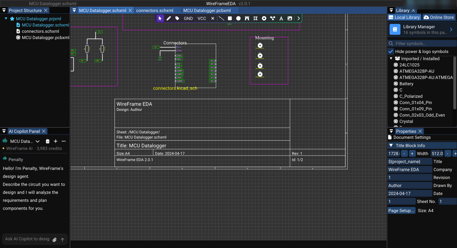
Click empty canvas to show Document Settings. Under Title Block Info set the Width and Height of the title block, Title, Company, Revision, Drawn By, Date, Sheet No., and Total. Size shows the current paper size; Page Setup... opens the full Page Settings dialog with paper size, border, and logo — see Templates and Title Block.
Complete these fields before PDF release so every exported sheet can be identified independently.
Component properties#
When one component is selected, review:
| Tab / section | Property | Purpose |
|---|---|---|
| General → Info | Designator | Unique circuit reference such as R1 or U3 |
| Value | Electrical value or part number used by design and BOM | |
| Comment | Supporting note when needed | |
| Exclude from PCB | Leaves the part out of Update Schematic to PCB | |
| General → Location | Position, Rotation | Placement on the sheet |
| General → Linked Footprint | Footprint, Link Footprint & Save to File | Physical package used by PCB update |
| 3D Model | — | Preview of the footprint's 3D model |
| Pins | No, Name, Show Num, Show Name | Pin numbering and which pin texts are shown |
The eye button beside Designator, Value, and Comment shows or hides that text on the sheet.
Moving and aligning component text#
- Right-click the component and choose Edit Attributes (Lock Body). The body stays put while you work on its texts.
- Drag the designator, value, or pin texts; rotate a selected text with Space (or R); align several with Shift+Y / Shift+X.
- Right-click again and choose Finish Editing.
Sync Attributes to Similar Components (right-click) copies the position, rotation, size, and visibility of this component's designator, value, and pin texts to every component with the same value (or name) and the same footprint.
Wire and net properties#
Selecting a wire or net label exposes its net name and available connectivity information. Use consistent names for rails and signals; renaming a shared net can affect multiple labels and connected items.
Net classes for the PCB are set in Design Rules and Net Classes.
Multi-selection and graphics#
A selected graphic shows Graphic Object: Content for text, Size, Color, and Thickness, depending on its type.
After a bulk change, zoom in and inspect each affected item before saving.
Review checklist#
- Sheet revision and title match the release.
- Designators are unique.
- Values include necessary units and tolerances.
- Footprints match the exact package.
- Text is visible and does not obscure connectivity.
- Net names are consistent across the sheet.
- Structural changes are followed by ERC and PCB update review.