Start here
Getting Started
On this page
This guide walks you through your first session with WireFrame EDA in about 10 minutes: launching the application, the main window, and your first project.
What you'll learn
- Launching WireFrame
- Understanding the main window
- Creating a project
- Adding schematic and PCB files
- Opening existing projects and files
1. Launching WireFrame#
Open the Start menu → type WireFrame → press Enter.
Open Applications (or Launchpad) → WireFrame.
Open WireFrame EDA from the application menu.
No sign-in is needed: WireFrame runs in community mode. On startup it restores the window size and position, and reopens the projects and documents that were open when you quit (Preferences → Workspace → Restore on launch).
2. The Main Window#
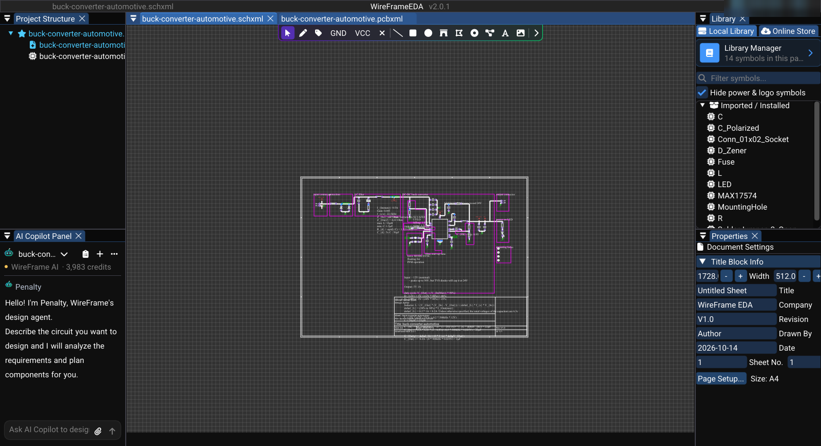
| Area | Default position | Purpose |
|---|---|---|
| Menu bar | Top | File, Edit, View, Tools, Simulation, Preferences, Help, and the account menu on the right |
| Project Structure | Left, top | Project file tree |
| AI Copilot | Left, bottom | Chat with the design assistant |
| Editor | Centre | One tab per open schematic or PCB |
| Library / Footprints | Right, top | Symbols for a schematic, unplaced footprints for a PCB |
| Properties | Right, bottom | The selected object, or the document settings |
| Layers (PCB) | Beside the Properties panel | Visibility, lock, and colour of PCB layers |
| Notifications | Bottom of the editor | Short messages such as Document saved successfully |
Rearranging panels
Drag any panel tab to another edge or corner. The layout is saved when you quit. Preferences → Reset to Default Layout puts every panel back; Preferences → Workspace → Layout presets saves arrangements under a name.
3. Creating a New Project#
Why use a project?
A project (.prjxml) links your schematics, PCBs, and project library. Update Schematic to PCB and AI design work need a project.
Steps:
- Go to File → New → New Project (.prjxml)...
- Choose the folder for the project (Select Folder for New Project).
- In Create New Project, type the project name and select Create.
WireFrame creates, in that folder:
<name>.prjxml— the project file with its list of schematics and PCBs;lib_<name>/— the project library, where repaired and generated parts are saved.
The Project Structure panel shows the new project. Right-click it to Add New Schematic or Add New PCB.
4. Adding a Schematic File#
- Right-click the project in Project Structure → Add New Schematic. Or use File → New → New Schematic (.schxml) (Ctrl+N) for a standalone sheet.
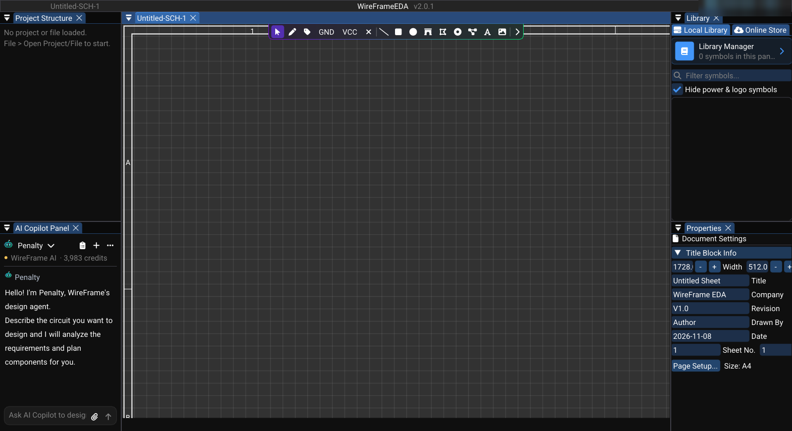
- A new tab opens in the editor. The canvas shows a dot grid, the page outline, rulers, and the schematic toolbar centred at the top.
- Press Ctrl+S to save it as a
.schxmlfile, for examplemain.schxml.
5. Adding a PCB File#
- Right-click the project → Add New PCB, or use File → New → New PCB (.pcbxml).
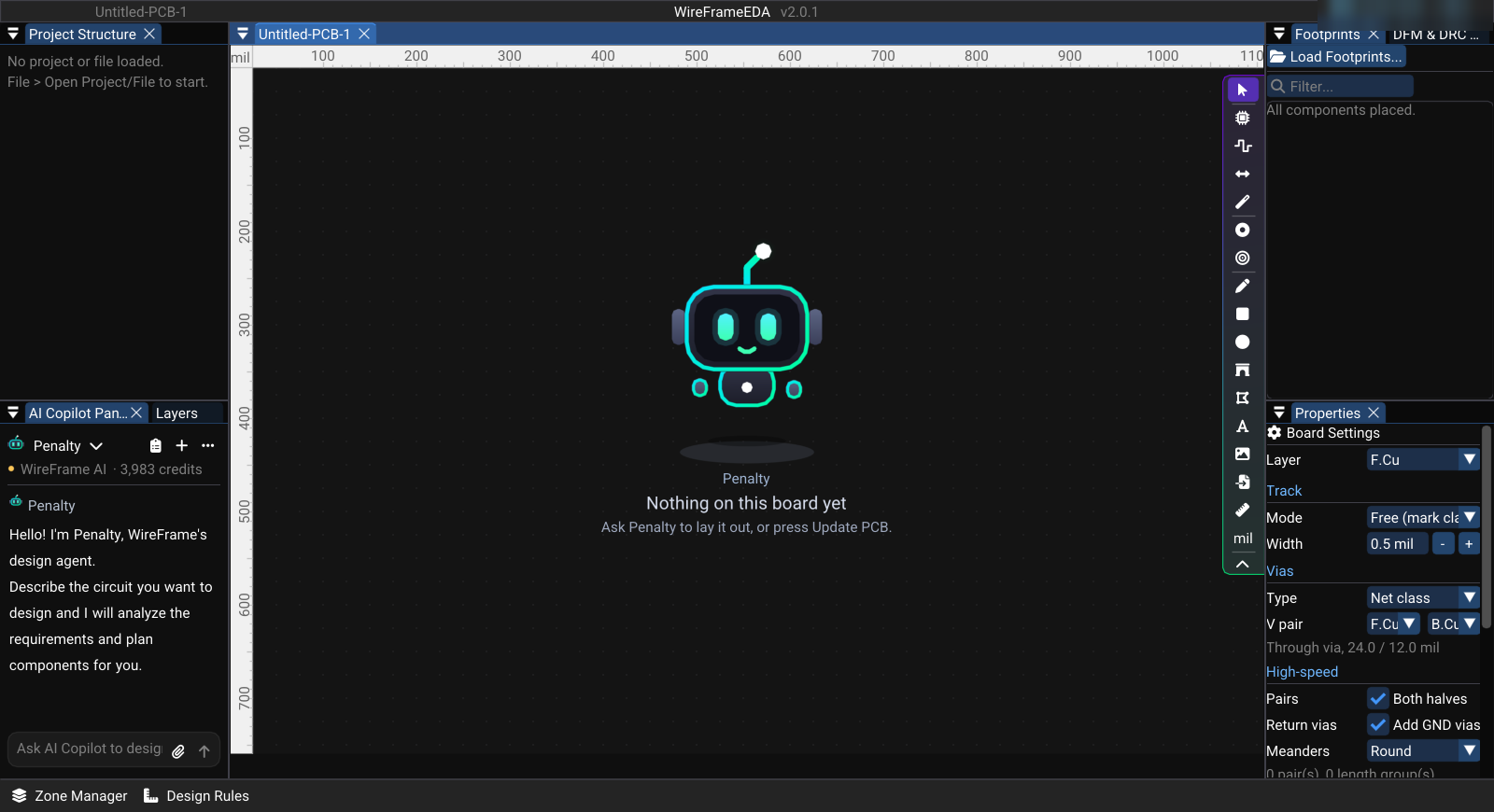
- A new tab opens with rulers, a grid, and the PCB toolbar on the right edge of the canvas.
Convert from schematic instead
Complete your schematic first and use Tools → Update Schematic to PCB. Footprints arrive on the board in a grid with their nets; review the target board, imported footprints, and ratsnest before routing.
6. Opening an Existing Project or File#
Opening a project (.prjxml)#
- File → Open Project (.prjxml)... (Ctrl+P)
- Select the
.prjxmlfile - The Project Structure panel lists its schematics and PCBs
- Click an entry to open it in the editor
Opening a single file#
- File → Open File... (Ctrl+O)
- Select a
.schxml(schematic),.pcbxml(PCB), or.prjxml(project) file - A schematic or PCB opens as a tab — no project required
Next Steps#
| Next page | Content |
|---|---|
| UI Overview | Every panel and menu |
| Schematic Editor | Place components, draw wires, manage nets |
| PCB Editor | Lay out footprints, route traces, export Gerbers |
| Full Tutorial | End-to-end walkthrough: a complete LED circuit |