Start here
User Interface Overview
On this page
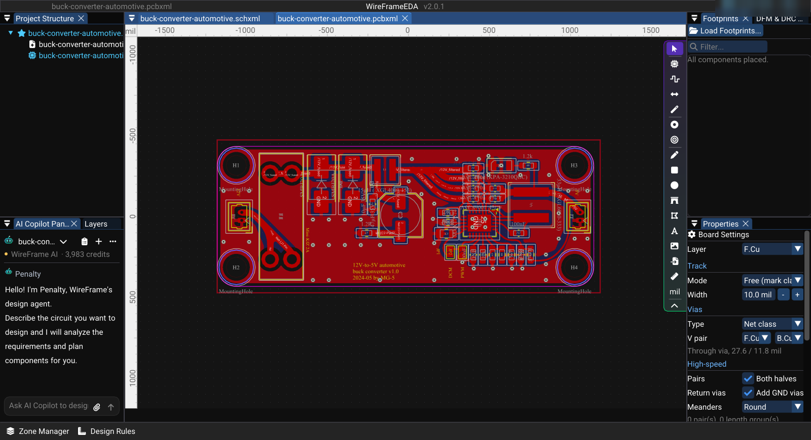
WireFrame uses dockable panels around the active schematic or PCB editor. Available tools and panels change with the active document type.
Main menus#
File#
Use File to:
- New — New Project (.prjxml)..., New Assembly (.asmxml)..., New Schematic (.schxml) (Ctrl+N), New PCB (.pcbxml), New Simulation (.simxml);
- Open File... (Ctrl+O), Open Project (.prjxml)... (Ctrl+P) and Open Assembly (.asmxml)...;
- Import — KiCad Project (.kicad_pro, .pro)..., Altium Project (.PrjPcb, .SchDoc, .PcbDoc, .zip)... and, with a PCB active, CAD Outline (.svg / .dxf)... — see Import and Export;
- Save (Ctrl+S) and Save As... (Ctrl+Shift+S);
- Export — Export Schematic to PDF..., Print PCB to PDF (1:1)..., Fabrication Outputs (Gerber/Drill/BOM)..., KiCad Project..., Altium Designer Project..., EasyEDA Project (Standard)...;
- Page Settings... for the active schematic;
- Close Document, Close Project, Close Assembly, and Exit.
Commands that do not apply to the active document are disabled.
Edit#
Use Edit for Undo, Redo, Cut, Copy, Paste, and Delete in the active editor. The shortcuts shown follow your key bindings.
View#
Use View to show or hide:
- Project Structure;
- Editor Panel;
- Component Library;
- Properties;
- Local Library Manager;
- AI Copilot Chat;
- PCB Layers;
- Zone Manager — see Zone Manager;
- Design Rules — see Design Rules;
- High-Speed Workbench — see High-Speed Workbench;
- Power Analyzer (DC IR drop) — see Power Analyzer;
- 3D Viewer (3);
- Assembly View — see Multi-Board Products;
- Schematic | PCB | 3D and Views as Tabs — see Side by Side;
- Performance HUD — a frame-time overlay; see the FAQ entry The canvas feels slow or stutters under Schematic and PCB.
Tools#
Use Tools for Symbol Library Editor, PCB Footprint Editor, Auto Wire, Update Schematic to PCB (a submenu when the project has several PCBs), Electrical Rules Check (ERC), DFM & DRC Check Panel..., Fabrication Output..., and Gerber Viewer.... Commands that do not apply to the active document are disabled.
Simulation#
Use Simulation for New Simulation (.simxml), Simulate a Block of This Sheet..., the SPICE Simulation Panel, Pre-flight Validation Checklist, and SPICE Model Editor. A simulation is a file of its own; sheets of the design are not simulated — see Get a simulation.
Preferences#
Preferences... (Ctrl+,) opens the Preferences dialog — see the categories below. Use Reset to Default Layout only when you intend to discard the saved docking layout.
Help and account#
The Help menu has Documentation (this guide), Report a Bug..., Request a Feature... (see Reporting an issue), Download Latest Version — or Update to v… when a newer version exists — and About WireFrame EDA.
The account menu at the right end of the menu bar shows who is signed in and the plan. It offers Sign in with browser (or Manage account, plan & devices and Sign out of this device once signed in), Star repository, Donate / Buy me a coffee and Check for Updates. See Account, Plans and Devices.
Light and dark#
Preferences → Appearance switches the whole app between Dark and Light — a soft-grey light theme with colours deepened to stay readable — and sets the accent colour, the interface font and its size. The schematic canvas has its own Auto / Paper / Dark choice: Auto follows the theme, Paper is a white sheet, Dark is the classic dark sheet.
Docking layout#
Drag a panel by its title to dock it to another edge or tab group. Preferences can enable detachable multi-monitor panels and companion-panel behavior.
Project Structure#
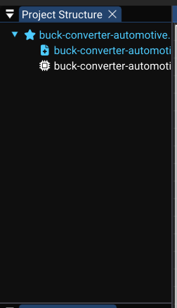
The Project Structure panel lists the open projects with their schematics and PCBs. Standalone files appear separately. Click a file to open it; Shift / Ctrl (Cmd on macOS) select several.
Right-click the project for Add New Schematic, Add New PCB, Rename Project, Open in Explorer, and Close Project. Right-click a file for:
| Item | What it does |
|---|---|
| Open, Reload | Open it, or read it again from disk |
| Rename, Open in Explorer | Rename the file, or show it in the system file manager |
| Set Root Schematic ▸ (PCB only) | Choose which schematic sheet this board is built from, or None (Clear Mapping) |
| Exclude from Project / Un-Exclude from Project | Keep the file listed but leave it out of the project's design |
| Remove from List | Take the file out of the project; the file stays on disk |
| Delete... | Delete the file from disk after a confirmation. This cannot be undone; open tabs of the file close and unsaved changes are lost. Del does the same for the selected files |
Editor panel#
The center editor displays the active schematic or PCB. Common actions include:
- mouse wheel to zoom;
- middle-drag or the configured pan action to move the view;
- click or box selection;
- context menu for object-specific actions;
- shortcuts shown in the active key map.
Toolbars change when switching between schematic and PCB documents.
Component Library#
With a schematic active, the Library panel has two tabs:
- Local Library — symbols from your library sources. Filter... searches, Hide Power/Logo hides power symbols and logos, and Manage libraries... opens the Library Manager. Drag a symbol onto the sheet to place it.
- Online Store — WireFrame's online component catalog. Install downloads a part with its symbol, footprint, and 3D model; Drag to schematic places an installed part.
With a PCB active, the panel becomes Footprints: the design's footprints that are not on the board yet, a Filter... box, and Load Footprints... to add a .kicad_mod file. Drag a row onto the board to place it.
Use View → Local Library Manager to add or remove library sources — see Library Import and Management.
Properties#
Properties follow the current selection:
- a library symbol selected in the Library panel shows a preview with Symbol, Footprint, and 3D Model tabs;
- a schematic component shows Component Properties with General, 3D Model, and Pins tabs;
- empty schematic canvas shows Document Settings (title block);
- a PCB footprint shows Footprint Properties — reference, value, position, rotation, Flip Layer (F);
- traces, vias, holes, and graphics show their own settings;
- nothing selected on a PCB shows Board Settings — active layer, track width, via type, high-speed options, corner style, and the rules of the active net.
Ctrl+E brings the Properties panel back if it is hidden.
PCB Layers#
The Layers panel sets the copper stackup, the active layer, and each layer's visibility, lock, and colour. Hiding a layer changes the view, not the board data. Confirm the active copper layer before routing or adding vias — see Layers and Views.
Notifications and logs#
Status messages and notification overlays report saves, imports, checks, and failures. Read the full message before repeating an action. For simulation, also inspect Last run and the simulation log.
Current Preferences categories#
| Category | Includes |
|---|---|
| General | Display units (Mil / Millimeter), autosave and its interval |
| Appearance | Theme mode (dark / light), accent colour, interface font, font file, and font size |
| Workspace | Detachable panels (drag panels onto another monitor), Companion panels follow their editor, Default layout, Restore on launch, Layout presets |
| Grid & Snap | Show grid, Crosshair at cursor, Snap to grid (hold Alt to place off-grid), Grid step |
| Editing | Rotate step for both editors; Default trace width (mil) for new boards |
| Keyboard Shortcuts | Key bindings — see Keyboard Shortcuts |
| Simulation | Default analysis, Transient defaults (stop time, time step), Engines (ngspice is built in; Xyce, LTspice, and an external ngspice are optional) |
| Libraries | Library Manager, online catalog, loaded sources, and the library cache folder |
| 3D Viewer | Materials of the 3D board preview: solder mask, trace under mask, pad plating, silkscreen |
| AI Assistant | WireFrame AI and your plan's AI credit left — see AI Copilot |
| Updates | Version, licence tier, and the update check |
A search box at the top finds settings by keyword.
Select OK to keep changes or Cancel to discard pending dialog changes.