PCB layout
Layers and Views
On this page
PCB layers control which drawing plane is active — copper, silkscreen, solder mask, or board outline. This page covers the layer stack, the Layer panel, rendering behavior, and canvas navigation.
Default Layer Stack#
| Layer | Color | Contains |
|---|---|---|
| F.Cu | Red | Front copper — traces and pads |
| B.Cu | Blue | Back copper |
| F.SilkS | Yellow | Front silkscreen — labels, outlines, logos |
| B.SilkS | Cyan | Back silkscreen |
| F.Mask | Translucent purple | Front solder mask openings (around pads) |
| B.Mask | Translucent cyan | Back solder mask openings |
| F.Paste | Translucent light grey | Front solder paste |
| B.Paste | Translucent grey | Back solder paste |
| F.Fab | Grey | Front fabrication layer |
| B.Fab | Dark grey | Back fabrication layer |
| F.CrtYd | Light grey | Front courtyard (keep-out area per component) |
| B.CrtYd | Light grey | Back courtyard |
| Edge.Cuts | Magenta | Board outline — physical board shape |
| Dwgs.User | White | User drawings and notes |
| Eco1.User, Eco2.User, Cmts.User | Green, olive, blue | Extra user layers |
Boards with more than two copper layers add inner layers (In1.Cu, In2.Cu, …) between F.Cu and B.Cu.
The Layer Panel#
Open View → PCB Layers. The Layers panel follows the active PCB:
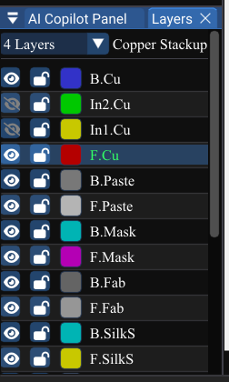
| Control | Interaction |
|---|---|
| Copper Stackup | Number of copper layers: 2, 4, 6, 8, 16, or 32 Layers |
| Hide All References | Hides every footprint designator on the canvas |
| Vis (eye) | Click to show / hide the layer |
| Lock | Click to lock the layer; hover shows Layer Locked or Click to lock layer |
| Color | Click the swatch to change the layer color |
| Name | Click to make it the active layer |
The active layer has a highlighted background.
Locked layers#
Footprints, traces, and designators on a locked layer ignore clicks, so they cannot be selected or moved by accident, and changing layer onto it while routing is refused with "… is locked". Lock finished layers — the board outline, for instance — to protect them while you work on the rest.
The Active Layer#
The active layer determines where traces and graphics are placed:
- Routing a trace → places it on the active copper layer
- Drawing text → places it on the active layer (set to F.SilkS for silkscreen labels)
- Change the active layer by clicking its name in the Layers panel, or from the keyboard: Tab (to its via pair, F.Cu ↔ B.Cu by default), = / - (next / previous copper layer), Page Up / Page Down (F.Cu / B.Cu). A short note on the canvas confirms Active layer: …
Always check your active layer before routing
F.Cu (red) and B.Cu (blue) are physically different sides of the board. Routing on the wrong layer will not connect the intended pads.
Hiding and Showing Layers#
Click the eye icon next to a layer name to toggle its visibility:
- Hidden layers — traces, pads, and graphics are not drawn on the canvas
- The data still exists on the board and in the saved file — hiding a layer does not remove anything
Practical examples:
- Hide B.Cu while working on the front side to reduce visual clutter
- Hide F.SilkS to inspect trace routing without text overlay
- Re-enable all layers to review the full board
Changing Layer Colors#
Click the color swatch next to any layer name to open a color picker.
Default colors are chosen for easy visual distinction (red/blue for copper). You can adjust them to your preference.
How Colors Render on the Canvas#
| Element | Color source |
|---|---|
| Trace | The layer the trace is on |
| Pad | Copper layer color |
| Footprint graphics | Layer of each individual graphic (SilkS, Fab, etc.) |
| Silkscreen | F.SilkS or B.SilkS layer color |
| Board outline | Edge.Cuts layer color |
| Copper zone | Layer color rendered semi-transparently |
Canvas Navigation#
| Action | Input |
|---|---|
| Pan | Middle-drag or right-drag; two-finger scroll on a macOS trackpad |
| Zoom in / out | Scroll wheel, centred on the cursor (Ctrl / Cmd + scroll on macOS) |
| 100% zoom | Ctrl+0 |
| Toggle grid / crosshair | Shift+G / Shift+C |
| Switch unit mm / mil | Shift+U, or the mil / mm button on the toolbar |
Fit to Screen (Home) and Zoom to Selection (Ctrl+Shift+F) work in the schematic editor only.
See Also#
- PCB Editor Overview — general PCB workspace
- Routing — the active layer determines which copper layer is routed
- Fabrication & Export — layer selection for Gerber export