Schematic
Schematic Editor — Overview
On this page
The Schematic Editor is where you design your circuit: place components, draw wires, assign net labels, and prepare for PCB layout.
What You Can Do Here#
| Task | Tool |
|---|---|
| Place components from libraries | Drag a symbol from the Library panel onto the sheet |
| Draw wires connecting pins | Wire tool (W) |
| Assign net labels (SDA, SCL, +3V3…) | Label tool (N) |
| Place power symbols (GND, VCC) | Place GND (G) / Place VCC (P) |
| Draw annotations (boxes, text, lines) | Line, Rect, Text tools |
| Edit component properties | Properties panel |
| View net connectivity | Built automatically as you draw |
Workspace#
The schematic workspace consists of:
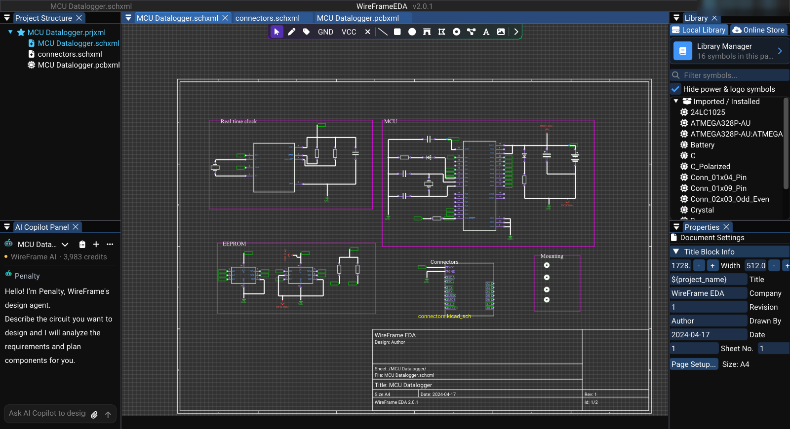
- Canvas — dot grid with an A4 page outline (configurable to A3, custom). Place all components and wires here.
- Toolbar — a strip of tool buttons centred at the top of the canvas; Tab hides or shows it
- Library panel — symbol list for placing components
- Properties panel — edit properties of the selected item or page settings
- ERC panel — electrical rules check results (details)
- Simulation panel — configure and run SPICE simulations (details)
Toolbar Modes#
Each toolbar button activates a drawing mode that determines how mouse clicks are interpreted:
| Tool (tooltip) | Shortcut | Behavior |
|---|---|---|
| Select | Esc | Click to select, drag to move, drag a box to multi-select |
| Wire | W | Click to start / add corners / end a wire |
| Label | N | Click to place a net label |
| Probe Signal | V | Click a wire, pin, net label, or power symbol to place a probe marker on its net for the simulation — see Waveform Viewer |
| Place GND | G | Click to place a GND power symbol |
| Place VCC | P | Click to place a VCC power symbol |
| Draw Line | Shift+L | Click start → drag → release |
| Draw Rectangle | R | Click one corner → drag to opposite |
| Draw Circle | E | Click center → drag to set radius |
| Draw Arc | A | Click to define arc points |
| Draw Polygon | O | Click vertices → right-click to close |
| Junction | J | Click to place junction dots manually |
| Net Harness | H | Drag to draw a harness line — a drawing that marks a bundle of signals; it does not connect nets |
| Place Text | T | Click to place a text annotation |
| Import Image | — | Place a PNG, JPG, or BMP picture at the centre of the view |
The active tool is highlighted cyan. Press Esc to return to Select mode at any time.
Basic Interactions#
Selecting objects#
| Action | Input |
|---|---|
| Select a single component | Left-click on it |
| Select multiple objects | Drag a selection box on empty canvas |
| Open context menu | Right-click any object |
| Cancel current operation | Esc |
| Delete selected | Del or Backspace |
| Undo / Redo | Ctrl+Z / Ctrl+Y |
Smart interactions#
- Dragging a component — connected wires follow automatically, no broken connections
- Rotating (Space, or R with a component selected) — the component rotates by the rotation step (90° by default), wires adjust to the new pin positions
- Deleting a component — connected wires are also removed (fully undoable)
Section Pages#
Continue to the detailed guides for each aspect of schematic design:
| Page | What you'll learn |
|---|---|
| Placing Components | Load libraries, place symbols, edit designators |
| Wiring & Nets | Draw wires, connect pins, net labels, GND/VCC |
| Properties & Attributes | Edit page settings, component attributes, text |
| Graphics & Annotations | Draw boxes, lines, annotations |
| ERC (Electrical Rules Check) | Validate connectivity before PCB conversion |
| Templates & Title Block | Page setup, title block customization |
Related Sections#
| Section | What you'll learn |
|---|---|
| Simulation | Run SPICE simulation on your schematic |
| Symbol Library Editor | Create or correct custom schematic symbols |
| AI Copilot | Generate schematics from text descriptions |