PCB layout
PCB Editor — Overview
On this page
The PCB Editor handles board layout — from component placement to trace routing, copper zones, design rule checks, and manufacturing file export.
What You Can Do Here#
| Task | Tool |
|---|---|
| Bring footprints in from the schematic | Tools → Update Schematic to PCB |
| Place a footprint again after removing it | Drag it from the Footprints panel |
| Route copper traces between pads | Route Trace (X) |
| Place vias to switch routing layers | Place Via (V), or V while routing |
| Add mechanical holes (screws, standoffs) | Place Mounting Hole (H) |
| Define the board outline | Edge.Cuts layer + drawing tools, or File → Import → CAD Outline |
| Fill copper zones (ground planes) | View → Zone Manager |
| Set clearances, widths, and net classes | View → Design Rules |
| Run DFM / DRC checks | Tools → DFM & DRC Check Panel... |
| Export Gerber, drill, BOM, PDF | File → Export → Fabrication Outputs (Gerber/Drill/BOM)... or Tools → Fabrication Output... |
| Preview the board in 3D | View → 3D Viewer (3) |
Workspace#
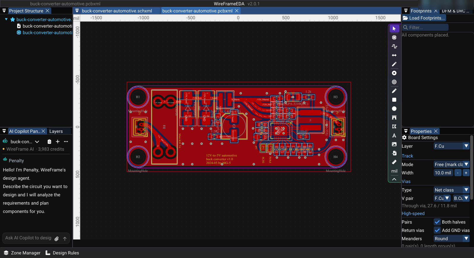
- Canvas — the board area with rulers, grid, footprints, traces, zones, and ratsnest lines (unrouted connections)
- Toolbar — a vertical strip of tool buttons on the right edge of the canvas; Tab hides or shows it
- Layers panel — toggle visibility and select the active layer (View → PCB Layers)
- Footprints panel — footprints of the design that are not on the board yet
- Properties panel — the selected object, or Board Settings when nothing is selected
PCB Toolbar Tools#
From top to bottom:
| Tool | Shortcut | Function |
|---|---|---|
| Select | Esc | Select and move objects |
| Place Footprint | O | Footprints are placed by dragging them from the Footprints panel |
| Route Trace | X | Route copper traces between pads — see Routing |
| Tune Length | — | Add meanders to a net that is shorter than its target — see Routing |
| Place Via | V | Place a via by itself |
| Place Mounting Hole | H | Place a mechanical hole |
| Draw Line / Rectangle / Circle / Arc / Polygon | Shift+L / R / E / A / — | Draw shapes on the active layer |
| Place Text | T | Place text on the active layer |
| Vectorize Image | — | Turn a PNG/JPG logo into board artwork — see below |
| Import CAD (SVG) | — | Import an SVG drawing — see Board Shape and Outline |
| Measure | M | Place a dimension: click the start, click the end, move to set the offset, click to place |
| mil / mm | Shift+U | Switch the display unit |
Board Outline (Edge.Cuts)#
Every PCB needs a board outline that defines its physical shape:
- In the Layers panel, click Edge.Cuts to make it the active layer
- Use the Draw Rectangle (or Polygon) tool to draw the board shape
- The outline appears in magenta
You can also import a mechanical drawing — see Board Shape and Outline.
Why Edge.Cuts matters
The board outline is used for: - Telling the manufacturer where to cut the board - Defining the valid placement area for footprints (DFM checks this) - Clipping copper zone fills at the board edge
Ratsnest Lines#
Ratsnest lines are thin dashed lines showing connections that have not yet been routed:
- Ratsnest lines automatically update after every edit
- When you route a trace, the corresponding ratsnest line disappears
- The goal is to route until all ratsnest lines are gone
Logos and Images#
Vectorize Image on the toolbar turns a PNG, JPG, or BMP into board artwork:
- Choose the image. Image Vectorizer Settings opens with a Live Preview.
- Adjust Invert Colors (for light art on a dark background), Fill Style (None (Outline), Solid Fill, Hatch (Grid)), Threshold (Black/White) — or Auto to pick it — Smoothing, Edge Blur, and Simplification (Epsilon).
- Set the size with Scale (mils per pixel) or Target Width (mm); Size Info shows the result in mm and mil.
- Select Import. The artwork is added on F.SilkS as a footprint named
LOGO…and follows the cursor — click to drop it. Move or rotate it like any other footprint.
Measure the result and check the line width against your manufacturer's minimum silkscreen or copper width before release.
Section Pages#
| Page | What you'll learn |
|---|---|
| Footprints & Placement | Load libraries, place and arrange footprints |
| Routing | Route traces, vias, mechanical holes |
| Layers & Views | Layer management, visibility, navigation |
| Zones & Planes | Copper fills, ground planes, zone priority |
| Design Rules & Net Classes | Clearance, trace width, via size, net class configuration |
| DFM & DRC | Design rule and manufacturability checks |
| Fabrication & Export | Gerber, drill, BOM, PDF export |
Related Sections#
| Section | What you'll learn |
|---|---|
| 3D Viewer | Preview the PCB with 3D component models |
| Placement and Routing Assistant | Review AI-assisted placement and routing proposals |