Start here
Tutorial: An LED Chaser Board
On this page
This tutorial builds one complete board: an NE555 clock steps a 74HC4017 decade counter, and ten LEDs set in a ring light one after another. It has 25 parts — enough to practise every step of the workflow on a board you could order: project, libraries, schematic, ERC, PCB update, board outline, placement, routing, DFM/DRC, and the fabrication package. Allow about an hour.
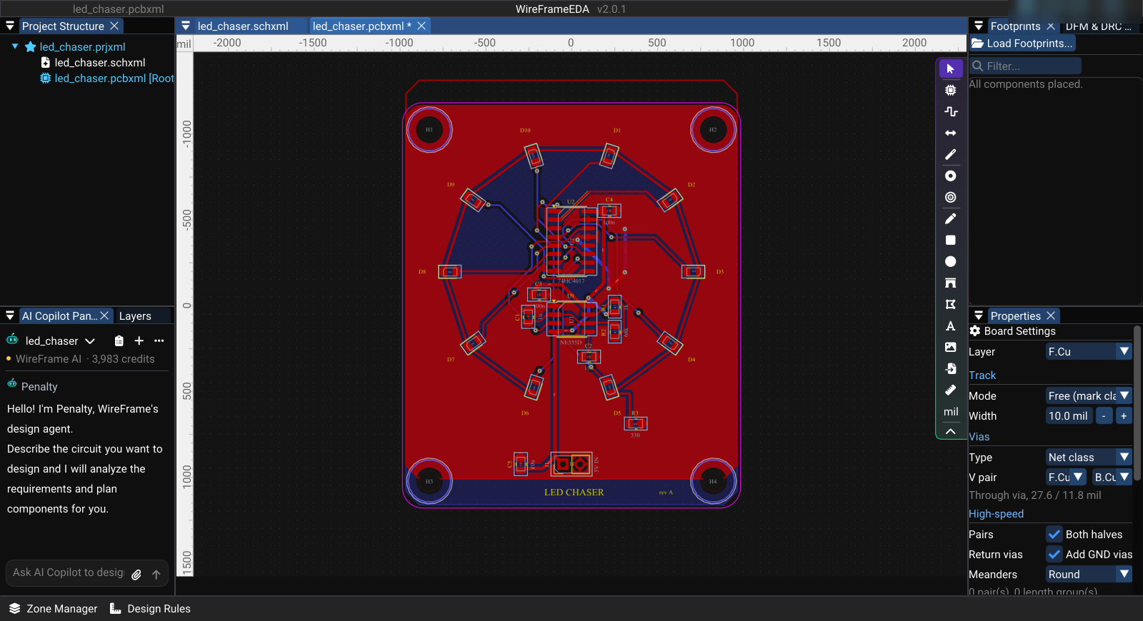
The finished project is in the documentation's samples, samples/led-chaser, at three stages — 1-schematic, 2-placed, and 3-routed. Open one with File → Open Project to compare it with your own work.
How the circuit works#
- U1, the clock. The NE555 runs as an astable oscillator. C1 charges through R1 and R2 and discharges through R2 alone, so the output toggles at f ≈ 1.44 / ((R1 + 2·R2)·C1) = 1.44 / ((1 kΩ + 136 kΩ) × 1 µF) ≈ 10.5 Hz. C2 (10 nF) steadies its CONT pin; RESET is tied to +5 V.
- U2, the counter. The 74HC4017 has ten outputs, Q0–Q9, and exactly one of them is high at a time; every rising edge on CLK moves it on, and after Q9 it starts again at Q0. CKEN and RESET are tied to GND so it counts freely. Cout (pin 12) is not used.
- D1–D10, the ring. Each output drives one LED's anode. Only one LED is lit at a time, so all ten cathodes share one resistor, R3, to GND: with a 5 V supply and a red LED dropping about 2.0 V, I ≈ (5 − 2.0) / 330 Ω ≈ 9 mA — a little less in practice, because the output itself drops a few tenths of a volt. That is well inside the 74HC4017's output rating. At about 10 steps a second, the light goes round the ring once a second.
- Supply. 5 V comes in on the 2-pin header J1. C5 (10 µF) holds up the input; C3 and C4 (100 nF) decouple each IC right at its supply pins.
The parts#
| Ref | KiCad symbol | Value | Footprint |
|---|---|---|---|
| J1 | Connector:Conn_01x02_Pin |
5V IN |
Connector_PinHeader_2.54mm:PinHeader_1x02_P2.54mm_Vertical |
| U1 | Timer:NE555D |
NE555D |
Package_SO:SOIC-8_3.9x4.9mm_P1.27mm |
| U2 | 4xxx:4017 |
74HC4017 |
Package_SO:SOIC-16_3.9x9.9mm_P1.27mm |
| R1, R2, R3 | Device:R |
1k, 68k, 330 |
Resistor_SMD:R_0805_2012Metric |
| C1, C2, C3, C4, C5 | Device:C |
1u, 10n, 100n, 100n, 10u |
Capacitor_SMD:C_0805_2012Metric |
| D1–D10 | Device:LED |
RED |
LED_SMD:LED_0805_2012Metric |
| H1–H4 | Mechanical:MountingHole |
— | MountingHole:MountingHole_3.2mm_M3 |
Add +5V, GND, and two PWR_FLAG symbols from the power library. The 4017 symbol is drawn for the CD4017; the 74HC4017 has the same pinout, and at 5 V it drives an LED much harder than a CD4017 can, so give the symbol the value 74HC4017.
| Net | Connects |
|---|---|
+5V |
J1.1, C5.1, U1.4 (RESET), U1.8 (VCC), R1.1, C3.1, U2.16 (VDD), C4.1 |
GND |
J1.2, C5.2, U1.1, C1.2, C2.2, C3.2, U2.8 (VSS), U2.13 (CKEN), U2.15 (RESET), C4.2, R3.2 |
DIS |
U1.7 (DISCH), R1.2, R2.1 |
THR |
U1.2 (TRIG), U1.6 (THRES), R2.2, C1.1 |
CV |
U1.5 (CONT), C2.1 |
CLK |
U1.3 (OUT), U2.14 (CLK) |
Q0 … Q9 |
U2 pins 3, 2, 4, 7, 10, 1, 5, 6, 9, 11 → the anode (pin 2) of D1 … D10 |
LED_K |
the cathode (pin 1) of D1 … D10, R3.1 |
| — | U2.12 (Cout): a no-connect flag |
Before you start#
- Create the project: File → New → New Project (.prjxml)..., choose an empty folder, type
led_chaserunder Enter Project Name, and select Create. - Make the parts available. The symbols are in KiCad's
Device,Timer,4xxx,Connector,Mechanical, andpowerlibraries, and the footprints inResistor_SMD,Capacitor_SMD,LED_SMD,Package_SO,Connector_PinHeader_2.54mm, andMountingHole. Add them in View → Local Library Manager (see Placing Components). The sample's KiCad source,samples/led-chaser/kicad, carries every footprint the board uses in itsfootprintsfolder.
1. Draw the schematic#
- Right-click
led_chaserin Project Structure → Add New Schematic, typeled_chaserin Create New File, and select Create: the sheet isled_chaser.schxml. - In the Library panel (Local Library tab), type each part's name in Filter... and drag it onto the sheet. Untick Hide power & logo symbols to find
PWR_FLAG. Rotate a part with Space while you place it. - Select each part and fill Properties → General → Info: Designator and Value from the table above. Check Linked Footprint; if it is empty, use Link Footprint & Save to File and pick the footprint from the table.
- Lay the sheet out in three groups, left to right — the supply, the clock, the counter with its LEDs — and wire each group with W: click a pin, click to add corners, and click the other pin to finish. To end on another wire or a free point, double-click.
- Draw the ten LEDs standing up in a row, anode at the bottom. Wire Q0 — the top output on the symbol — to the leftmost LED, Q1 to the next one, and so on to the right: then no two wires cross. Join the ten cathodes with one wire along the top, and take it through R3 to GND.
- Press G for each GND symbol and P for each supply symbol; set the supply's Value to
+5V. Put onePWR_FLAGon the+5Vwire and one on theGNDwire next to J1. - Press N and name the nets that a person will look for on the board:
CLK,DIS,THR,CV,LED_K, andQ0toQ9on the counter's outputs. The board's nets take these names, so a ratsnest line or a DFM message saysQ3instead of a generated name. - Press Q and click the end of U2 pin 12 (Cout) to mark it as left open on purpose.
- Save (Ctrl+S).
Check the LED orientation against the table: the anode (pin 2) goes to the counter, the cathode (pin 1) to the shared LED_K net.
Why PWR_FLAG
J1's pins are passive, so nothing on the sheet is typed as driving +5V or GND, while both ICs have power input pins on them. Without the flags ERC reports Input Power pin not driven by any Output Power pins on both rails. A PWR_FLAG says the rail is supplied — here, by the header.
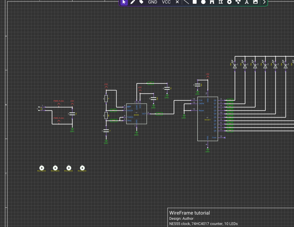
2. Check the schematic#
Select Tools → Electrical Rules Check (ERC). The window checks every sheet when it opens and groups what it finds by rule; Run ERC checks again after an edit. Click a row to see why it matters and how to fix it — the sheet moves to the place it names. A clean schematic reads ERC clean: nothing to report on any sheet.
Typical first-time findings on this board:
- Pin not connected — a wire stops short of a pin, or was never drawn. Draw it to the pin's end. If a pin is meant to stay open, like Cout, give it a no-connect flag (Q).
- Unconnected wire endpoint — a wire ends in empty space a little short of where it was aimed. Drag its end onto the pin or wire, or delete it.
- Input Power pin not driven by any Output Power pins — a
PWR_FLAGis missing (see the tip above).
Run the check again after each fix. A drawing that looks connected is not enough: ERC reads the connections, not the picture.
3. Bring the parts onto the board#
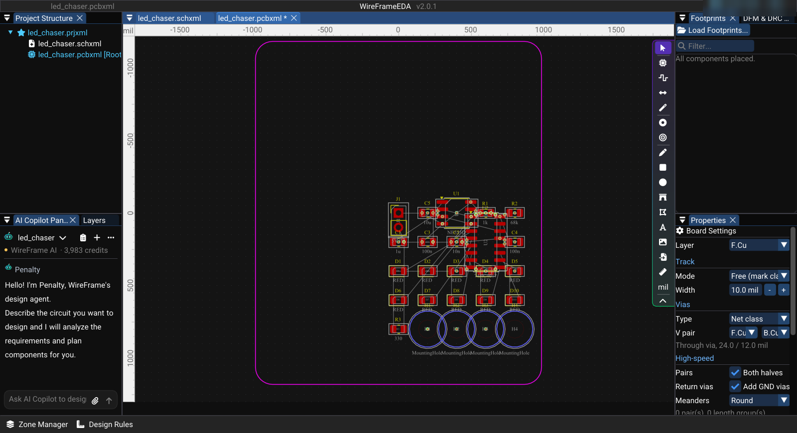
- With the schematic active, select Tools → Update Schematic to PCB. With no board in the project yet, WireFrame creates
led_chaser.pcbxml, makes this sheet its root, and brings in the 25 footprints in a grid, joined by ratsnest lines. A notification says the board has no outline yet. - Give the board its shape: File → Import → CAD Outline (.svg / .dxf)..., choose
led_chaser_outline.dxf(50 × 60 mm, 3 mm corners), tick Import as BOARD OUTLINE, and untick Center to Mouse Cursor so the board is centred on the origin. The verdict reads Board: 50.00 x 60.00 mm, 0 cutout(s); select Import. The holes come from H1–H4, so the outline has none. Other ways to set the shape are in Board Outline.
A board added by hand
If you add the board yourself first with Add New PCB, it has no root schematic yet, and Update Schematic to PCB stops with No Root Schematic mapped for this PCB. Right-click the board in Project Structure → Set Root Schematic → led_chaser.schxml, then update.
4. Place the parts#
Select each footprint and type its position into Properties → Footprint Properties → Transform (X and Y in mil, with mm beside them; Rotation in degrees). (0, 0) is the centre of the board and Y grows downward. The LEDs sit on a circle of 18 mm radius around (0, −5 mm), 36° apart, each with its anode pad facing the centre; the gaps at the top and bottom of the ring leave room for the supply to come in.
| Part | X (mm) | Y (mm) | X (mil) | Y (mil) | Rotation |
|---|---|---|---|---|---|
| D1 | 5.56 | −22.12 | 219 | −871 | 108° |
| D2 | 14.56 | −15.58 | 573 | −613 | 144° |
| D3 | 18.00 | −5.00 | 709 | −197 | 180° |
| D4 | 14.56 | 5.58 | 573 | 220 | −144° |
| D5 | 5.56 | 12.12 | 219 | 477 | −108° |
| D6 | −5.56 | 12.12 | −219 | 477 | −72° |
| D7 | −14.56 | 5.58 | −573 | 220 | −36° |
| D8 | −18.00 | −5.00 | −709 | −197 | 0° |
| D9 | −14.56 | −15.58 | −573 | −613 | 36° |
| D10 | −5.56 | −22.12 | −219 | −871 | 72° |
| U2 | 0.00 | −9.50 | 0 | −374 | 0° |
| C4 | 5.60 | −14.00 | 220 | −551 | 0° |
| U1 | 0.00 | 2.00 | 0 | 79 | 0° |
| C3 | −4.80 | −1.60 | −189 | −63 | 0° |
| R1 | 6.40 | 0.20 | 252 | 8 | −90° |
| R2 | 6.40 | 3.90 | 252 | 154 | −90° |
| C1 | −6.40 | 1.70 | −252 | 67 | −90° |
| C2 | 2.60 | 7.60 | 102 | 299 | 0° |
| R3 | 9.50 | 17.50 | 374 | 689 | 0° |
| J1 | −1.27 | 23.50 | −50 | 925 | −90° |
| C5 | −7.50 | 23.50 | −295 | 925 | −90° |
| H1 | −21.00 | −26.00 | −827 | −1024 | 0° |
| H2 | 21.00 | −26.00 | 827 | −1024 | 0° |
| H3 | −21.00 | 26.00 | −827 | 1024 | 0° |
| H4 | 21.00 | 26.00 | 827 | 1024 | 0° |
Then add ground on both layers: View → Zone Manager → GND plane ▾ → Top and bottom, then Refill.
5. Route and inspect#
- Click F.Cu in the Layers panel.
- Route the decoupling capacitor at the counter first, so it sits right at the pin it serves: press X, click C4 pad 1, and click U2 pin 16. Esc ends a route; Backspace takes back the last corner. While you route, the readout beside the pointer shows the net, its class, the width, and the clearance.
- Draw the cathode ring by hand — it is the board's signature: from D6's cathode to D7's, and on round the ring to D5, then to R3 pad 1. Leave the ring open at the bottom, between D5 and D6, so the supply can come in from J1.
- Let Auto-route do the rest: drag a selection box over the whole board and press Ctrl+Shift+W (Auto-route selection). It routes on both layers with vias, around the copper already there, as one undo step. The notification says how many connections it routed and names each one it left, with the reason. On this board it leaves one: U2 pin 15 to
GND, for the ground pour, which picks the pin up when the pours are refilled (View → Zone Manager → Refill). Route anything else it leaves by hand (see Route Assist), and let DFM/DRC confirm that nothing is unconnected. - Nets named
GNDor starting with+(+5V) use the Power class — 20 mil tracks, 15 mil clearance; the others use Default — 10 mil tracks, 6 mil clearance (see Design Rules). The LEDs draw under 10 mA, so either is ample.
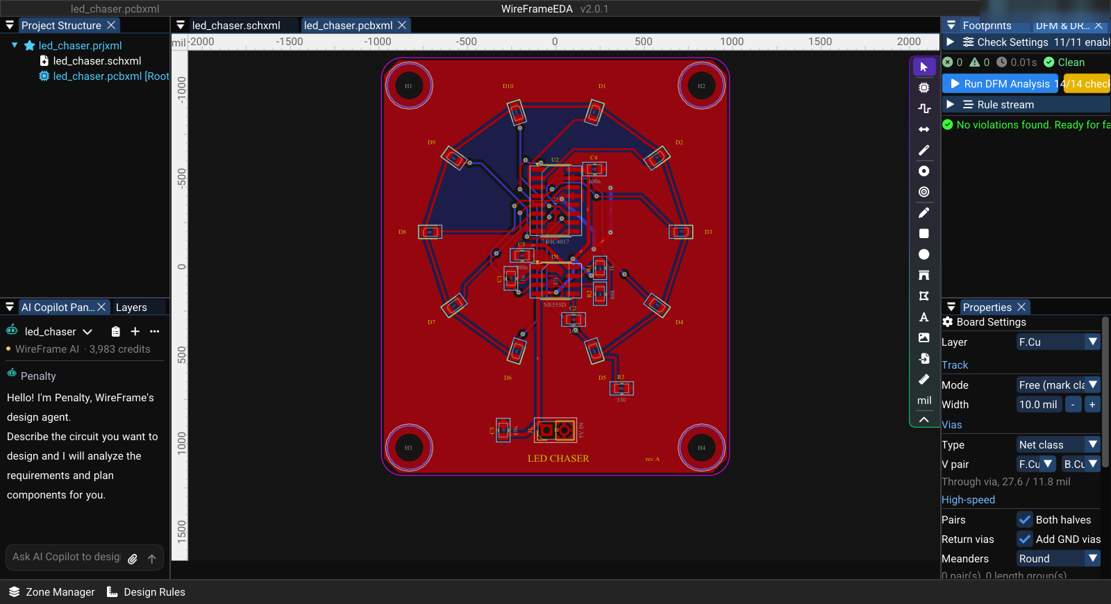
After routing, check the LED and connector orientation, that the silkscreen reads, and that no ratsnest line is left.
6. Run DFM/DRC#
Open Tools → DFM & DRC Check Panel... and select Run DFM Analysis. Click each error to jump to it, fix it, and run again until no error is left. Review each warning; record why an accepted warning is fine rather than hiding it. On the finished sample the panel reads Clean and No violations found. Ready for fabrication!
7. Generate the fabrication package#
- Save the board.
- Select File → Export → Fabrication Outputs (Gerber/Drill/BOM).... The Fabrication & Assembly Output window names the board, its size, its copper layers, and its revision.
- Set Revision to
A. It is written into every file, so two revisions cannot be mixed. - Select Generate & verify package. WireFrame refills the copper pours, writes every file, then reads each file back and checks it against the board object by object: The package matches the design means every pad, via, track, opening, and hole the board has is in the files, and nothing else is.
- Read the Files tab — copper, solder mask, paste, silkscreen, board outline, drill, and the BOM and placement files for assembly — and the Preview tab, which draws the Gerber and drill files themselves, layer by layer.
- Select Save package (.zip)... (or Save to folder...). Before you order, open the package in a full Gerber viewer as well (KiCad GerbView, gerbv, or your manufacturer's viewer).
Completion checklist#
- Project, schematic, and PCB are saved in the project folder.
- The LEDs' polarity is right (anode to the counter); every symbol has its footprint.
- ERC reports nothing; DFM/DRC shows no error.
- No ratsnest line is left, and both GND pours are filled.
- The package was generated and verified at revision
A, and you have looked at it in a Gerber viewer.