Schematic
Graphics and Annotations
On this page
Use schematic graphics and text to explain circuit intent, group related sections, and record design constraints. They support documentation but do not create an electrical connection unless the selected tool is explicitly electrical.
Choose the correct tool#
| Tool | Use it for |
|---|---|
| Draw Line (Shift+L), Draw Rectangle (R), Draw Circle (E), Draw Arc (A), Draw Polygon (O) | Visual grouping or explanatory shapes |
| Place Text (T) | Notes, limits, test points, and design intent |
| Net Harness (H) | A drawn line that marks a bundle of signals; it does not connect nets |
| Junction (J) | Explicit electrical meeting point of wires |
| Import Image | A PNG, JPG, or BMP picture (a logo, a block diagram) placed at the centre of the view |
Do not use a graphic line as a wire. If two pins must be electrically connected, use the Wire tool and verify the result with net highlighting or ERC.
Create and edit an annotation#
- Select the graphic or text tool.
- Place its points or bounds on the sheet.
- Press Esc when the shape is complete.
- Select it and use Properties → Graphic Object to set Content (text), Size, Color, or Thickness.
- Save and inspect the PDF result if the annotation is part of release documentation.
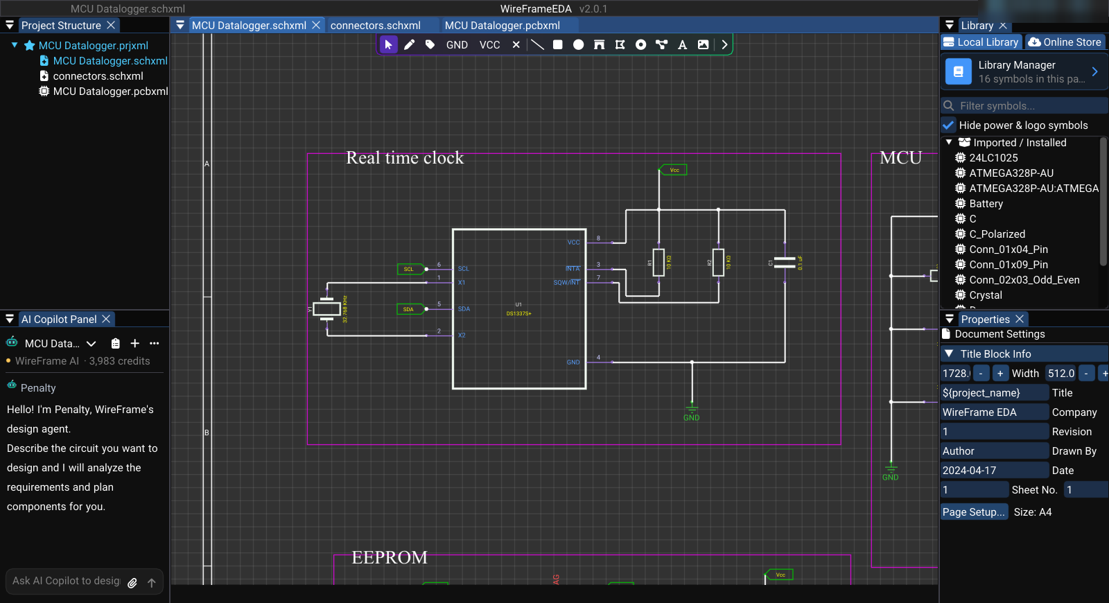
The KLP4e datalogger is a good model: every functional block on its main sheet — Real time clock, MCU, EEPROM, Connectors, Mounting — sits inside a rectangle with a title in large text. Imported from KiCad, those rectangles and titles come in as WireFrame graphics, drawn exactly where the author put them.
Annotation guidelines#
- State measurable constraints, not vague comments.
- Keep notes outside symbol pins and wires.
- Use consistent font size and restrained color.
- Include voltage, current, tolerance, or test conditions when relevant.
- Avoid duplicating information that is already controlled by a component property.
- Confirm that release-critical notes remain readable in exported PDF.
Dimensions#
The schematic editor has no dimension tool. Record required distances as text, and place real dimensions on the PCB with the Measure tool (M).