PCB layout
Fabrication and Export
On this page
Once the design is complete and DFM/DRC is clean, export the manufacturing package for your PCB manufacturer — or documents for review.
Export Types Overview#
| Output | Menu | Purpose |
|---|---|---|
| Fabrication package — Gerber X2, Excellon drill, BOM, pick-and-place, netlist, job file, README | File → Export → Fabrication Outputs (Gerber/Drill/BOM)... or Tools → Fabrication Output... | Everything a board house and an assembler need, as one .zip |
| Schematic PDF | File → Export → Export Schematic to PDF... | Printable schematic documentation |
| Print PCB to PDF (1:1) | File → Export → Print PCB to PDF (1:1)... | One true-scale PDF per layer, for review, toner transfer, or UV film |
The Fabrication Package#
- Save the board and run DFM & DRC.
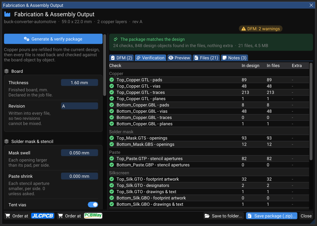
- With the PCB active, select File → Export → Fabrication Outputs (Gerber/Drill/BOM)... (or Tools → Fabrication Output...). The Fabrication & Assembly Output dialog opens.
- Open Options and check the settings (below).
- Select Generate Files to Memory. The dialog lists Generated n files with their sizes, and any warnings — for example No board outline on Edge.Cuts.
- Select Save Package (.zip)... and choose where to save. The default name is
Production_<date-time>.zip.
Nothing is written to disk until you save the package.
Options#
| Option | What it does |
|---|---|
| Solder mask swell (mm/side) | How much larger each mask opening is than its pad; 0.05 mm is the usual default |
| Paste shrink (mm/side) | Reduces every stencil aperture; leave at 0 unless your assembler asks |
| Board thickness (mm) | Finished thickness declared in the job file; 1.6 mm is the usual default |
| Revision | Written into every file's Gerber attributes and the job file, so the fab can tell revisions apart |
| Tent vias (cover with solder mask) | On: vias are covered. Off: the mask is opened over every via |
| Include netlist attributes (Gerber X2) | Adds net metadata so CAM can extract and verify the netlist |
| IPC-D-356A netlist (bare-board test) | Lets the fab flying-probe the bare board against this design |
| Assembly / documentation layers | Plots F.Fab, B.Fab, Dwgs.User, and Cmts.User when they contain anything |
| Job file (.gbrjob) | Gerber job file describing the stackup and the files |
| README manifest | Inventory of the package with the WireFrame version and generation time |
| Grouped BOM | Adds a BOM grouped by value and footprint |
| Drill report | Text summary of the drill tools |
What the package contains#
| File | Content |
|---|---|
Top_Copper.GTL, Bottom_Copper.GBL, ….G1, ….G2 … |
Copper layers (inner layers numbered from the top) |
Top_Mask.GTS, Bottom_Mask.GBS |
Solder mask openings |
Top_Paste.GTP, Bottom_Paste.GBP |
Stencil apertures |
Top_Silk.GTO, Bottom_Silk.GBO |
Silkscreen |
Board_Outline.GKO |
Board outline from Edge.Cuts |
Drill_PTH.DRL, Drill_NPTH.DRL |
Excellon drill files — plated and non-plated holes separately |
Top_Assembly.GM1, Bottom_Assembly.GM2, Drawings.GM3, Comments.GM4 |
Assembly and documentation layers, when enabled and not empty |
BOM.csv |
Columns Designator, Value, Footprint, Layer |
BOM_Grouped.csv |
Columns Comment, Designator, Footprint, Quantity, Layer, when Grouped BOM is on |
PickAndPlace.csv |
Component positions (CPL) for assembly |
<project>.d356 |
IPC-D-356A netlist, when enabled |
<project>.gbrjob |
Job file, when enabled |
Drill_Report.txt, README.txt |
Reports, when enabled |
BOM rows
The BOM lists every footprint that has pads or a value — mounting holes and logos without either are left out. Make sure every component has a Value before exporting.
Which files to send?
Most board houses take the whole .zip. Always check your manufacturer's requirements.
Schematic PDF Export#
- Open any schematic of the project.
- Select File → Export → Export Schematic to PDF....
- Choose a file name (default
schematic.pdf) and save.
Every schematic sheet of the project is exported into the one PDF, active sheet first. Sheets open in WireFrame are printed as you see them, including unsaved changes. Colours are kept; very light colours (white wires, pale yellow) are darkened so they print on white paper. The PDF includes symbols, wires, junctions, labels, graphics, and the title block.
Print PCB to PDF (1:1) — review, toner transfer, and UV film#
- With the PCB active, select File → Export → Print PCB to PDF (1:1).... The Export PCB to PDF dialog opens.
- Under Layers, tick the layers to print — each layer becomes its own PDF file.
- Set the Options:
- Include board outline (Edge.Cuts) on every page;
- Black & white — off prints each layer in its layer colour;
- Mirror — for toner transfer, mirror the top layers (F.Cu, F.SilkS); bottom layers are already seen through the board;
- Drill holes — punches pad, via, and mounting holes white with a thin ring so the drill bit has a centre to find.
- Select Export... and choose a folder. The files are written to
<project>_PDFs/<project>_<layer>.pdf, and a notification says how many were exported. - Print at 100% — never Fit to page. Each page carries a 10 mm bar; measure it on the printout before transferring.
Check the Gerbers before ordering#
Always look at the exported Gerber and drill files in a Gerber viewer before sending them to a manufacturer — it is the last chance to catch a missing layer, a shifted drill file, or an outline that did not export.
- Unzip the package and open the files in a full Gerber viewer: KiCad GerbView, gerbv, or the viewer on your manufacturer's order page.
- Load every copper, mask, silkscreen, outline, and drill file together.
- Check that:
- every layer you expect is present and aligned with the others;
- traces are continuous and pads sit on their copper;
- drill hits land in the centre of pads and vias;
- the board outline is closed and matches the mechanical drawing.
Built-in Gerber Viewer is a preview
Tools → Gerber Viewer... opens a .gbr (or .gtl, .gbl, .gts, .gbs, .gto, .gbo, .gm1) file in a WireFrame window. In the current release it shows the file name but does not yet draw the layer geometry, and it has no zoom or pan. Do not use it to approve a fabrication package — use one of the viewers above.
Complete Export Workflow#
- Run DFM/DRC and resolve every release-blocking error.
- Set Revision and the other options, then generate the package.
- Read the warnings in the dialog.
- Review the Gerber layers and both drill files in a viewer.
- Check the IPC-D-356A netlist, BOM, pick-and-place, and README.
- Archive only the verified board revision and send that archive to the manufacturer.
Inspect the archive
A successful export does not prove manufacturability. Confirm that Edge.Cuts is closed, drill classifications are correct, every expected layer is present, and the package matches the board revision being released.
See Also#
- DFM & DRC — run checks before exporting
- Layers & Views — what each layer contains
- File Formats — formats WireFrame reads and writes