PCB layout
DFM and DRC Checks
On this page
Before exporting Gerber files, run the DFM & DRC Check to find design-rule and manufacturability problems. DFM (Design For Manufacturability) checks that the board can be made; DRC (Design Rule Check) checks it against your net classes and constraints.
Fix errors before exporting
Do not export Gerber files while errors (red) remain. Manufacturers may reject the order, or the board may be defective.
Running the Check#
- With a PCB active, open Tools → DFM & DRC Check Panel... (or Run DRC in the Design Rules Manager).
- Optionally open Check Settings and choose which checks run (below).
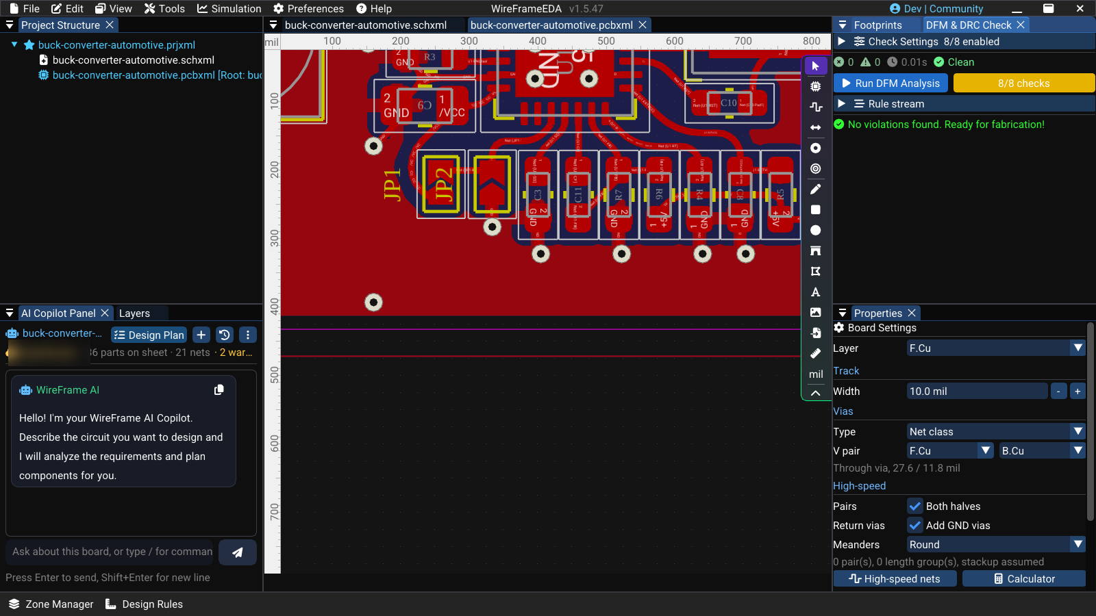
- Select Run DFM Analysis. A progress bar counts the finished checks, and Rule stream lists each step as it runs.
- The result line reads Found n Error(s) | n Warning(s), with errors listed first.
Check Settings#
The Check Settings header shows how many of the eight check groups are on (for example 8/8 enabled).
| Check | Looks for |
|---|---|
| Outline | A closed board outline on Edge.Cuts; copper too close to the board edge |
| Width | Tracks narrower than the fab minimum, or outside their net class width |
| Clearance | Copper of different nets too close together |
| Drill | Drill and via sizes, annular rings, hole-to-hole spacing |
| Nets | Missing connections (ratsnest lines left) |
| Orphans | Traces with a wrong or missing net |
| Placement | Overlapping component bodies, parts too close to the edge, artwork over parts |
| Missing | Components of the schematic that are not on the board |
Skip GND Conn turns off Nets and Orphans — useful while the GND zone is not filled yet. Enable All turns every check back on. Run the full set before release.
Reading the Results#
Each row shows an icon, a code, and a message, for example [E05] Clearance Error ….
| Code | Severity | Meaning |
|---|---|---|
| E00 | Error | Component in the schematic but not on the board |
| E01 | Error | Board outline missing on Edge.Cuts, or a track narrower than the fab minimum |
| E02 | Error | Unconnected net (ratsnest left), or a via drill below the fab minimum |
| E03 | Error | Via diameter below the fab minimum |
| E05 | Error | Clearance: copper of different nets too close. The two halves of a differential pair may sit at the class's pair gap when it is narrower than the clearance, and a pad with its own clearance (its own or its footprint's) is held to that instead of the class's — both as KiCad's DRC does |
| E06 | Error | Component bodies overlap |
| E07 | Error | A track or a pad too close to the board edge, measured against the board's real shape (notches and cutouts too), once per pad |
| E08 | Error | Annular ring of a via or pad below the minimum |
| E09 | Error | Two holes closer than the hole-to-hole minimum (a slot is measured as the slot it is; microvias are not mechanical holes) |
| E10 | Error | Solder mask bridge: the mask openings of two pads of different nets meet (closer than the board's minimum web), or an opening bares a track of another net. The openings are the pads grown by their own mask margin or the board's Mask swell |
| W01 | Warning | Track narrower than its net class |
| W02 | Warning | Via smaller than its net class |
| W05 | Warning | Orphaned track (wrong or missing net) |
| W06 | Warning | Graphics or a logo over a part, or parts under a plug-in module |
| W07 | Warning | Pads of an edge-mounted part (edge connector, castellation) at the board edge |
| W10 | Warning | Track wider than its net class maximum |
| W11 | Warning | Net length outside its class target ± tolerance |
| W12 | Warning | Differential pair skew over its budget |
| W13 | Warning | Track width does not give the class impedance target on this stackup |
| W14 | Warning | Length-matched group spread over its tolerance |
| W15 | Warning | High-speed via leaves a long stub |
| W16 | Warning | The two halves of a pair change layer a different number of times |
| W17 | Warning | High-speed net without a reference plane on the next layer |
| W18 | Warning | Two holes drilled on the same centre (a via dropped in a through-hole pad) |
| W19 | Warning | Custom rules from a KiCad .kicad_dru that WireFrame does not read (and so does not apply), or reads but does not check yet — named once, so a clean list is not read as "the board's rules passed" |
The limits come from Design Rules → Constraints and the net classes — see Design Rules.
Changing a severity#
Right-click a row to Change to Warning (or Change to Error) for this result, or Reset Severity to Default. Record why a downgraded item is acceptable; do not hide real problems to get a clean report.
A board imported from KiCad keeps the severities its designer set in the project (rule_severities): a check set to warning reports as a warning, one set to ignore is not reported, and the progress list says how many results each check left out ("ignored by board rules"). They are saved with the board and written back when it is exported to KiCad.
The project's custom rules (.kicad_dru) come with it too, kept as written. WireFrame applies a rule's hole size, via diameter and clearance when it understands every part of its condition — the rule areas an item touches, its net class, a differential pair, its type — and lists the rest under W19. The board's solder mask settings (mask swell, minimum web, whether one part's openings may meet) come from KiCad's board setup and are the ones the Fabrication window plots.
AI Explain Violations#
AI Explain Violations sends the current list to the configured AI and shows an explanation and an impact score (Impact n/5) under each row. It needs an AI endpoint (see AI Copilot); the explanation is advice, not a fix.
Viewing and Fixing Violations#
- Click a row — the canvas pans and zooms to the location (the tooltip shows its X / Y).
- Fix the issue: reroute, move the part, change the net class, or correct the outline.
- Select Run DFM Analysis again and repeat until no error remains.
With the panel open, markers on the canvas show where violations are. They hide while you edit and come back when the board has been still for a moment, so a marker never points at a part that has moved.
See Also#
- Routing — fix clearance and width violations
- Design Rules & Net Classes — the limits the checks use
- Zones & Planes — fill zones before checking connectivity
- Fabrication & Export — export after a clean check
- ERC — the schematic-side equivalent